SBOSA71 July   2021 TMCS1107-Q1

PRODUCTION DATA  

  1. Features
  2. Applications
  3. Description
  4. Revision History
  5. Device Comparison
  6. Pin Configuration and Functions
  7. Specifications
    1. 7.1  Absolute Maximum Ratings
    2. 7.2  ESD Ratings
    3. 7.3  Recommended Operating Conditions
    4. 7.4  Thermal Information
    5. 7.5  Power Ratings
    6. 7.6  Insulation Specifications
    7. 7.7  Safety-Related Certifications
    8. 7.8  Safety Limiting Values
    9. 7.9  Electrical Characteristics
    10. 7.10 Typical Characteristics
      1. 7.10.1 Insulation Characteristics Curves
  8. Parameter Measurement Information
    1. 8.1 Accuracy Parameters
      1. 8.1.1 Sensitivity Error
      2. 8.1.2 Offset Error and Offset Error Drift
      3. 8.1.3 Nonlinearity Error
      4. 8.1.4 Power Supply Rejection Ratio
      5. 8.1.5 Common-Mode Rejection Ratio
      6. 8.1.6 External Magnetic Field Errors
    2. 8.2 Transient Response Parameters
      1. 8.2.1 Slew Rate
      2. 8.2.2 Propagation Delay and Response Time
      3. 8.2.3 Current Overload Parameters
      4. 8.2.4 CMTI, Common-Mode Transient Immunity
    3. 8.3 Safe Operating Area
      1. 8.3.1 Continuous DC or Sinusoidal AC Current
      2. 8.3.2 Repetitive Pulsed Current SOA
      3. 8.3.3 Single Event Current Capability
  9. Detailed Description
    1. 9.1 Overview
    2. 9.2 Functional Block Diagram
    3. 9.3 Feature Description
      1. 9.3.1 Current Input
      2. 9.3.2 Input Isolation
      3. 9.3.3 High-Precision Signal Chain
        1. 9.3.3.1 Lifetime and Environmental Stability
        2. 9.3.3.2 Frequency Response
        3. 9.3.3.3 Transient Response
      4. 9.3.4 Internal Reference Voltage
      5. 9.3.5 Current-Sensing Measurable Ranges
    4. 9.4 Device Functional Modes
      1. 9.4.1 Power-Down Behavior
  10. 10Application and Implementation
    1. 10.1 Application Information
      1. 10.1.1 Total Error Calculation Examples
        1. 10.1.1.1 Room Temperature Error Calculations
        2. 10.1.1.2 Full Temperature Range Error Calculations
    2. 10.2 Typical Application
      1. 10.2.1 Design Requirements
      2. 10.2.2 Detailed Design Procedure
      3. 10.2.3 Application Curve
  11. 11Power Supply Recommendations
  12. 12Layout
    1. 12.1 Layout Guidelines
    2. 12.2 Layout Example
  13. 13Device and Documentation Support
    1. 13.1 Device Support
      1. 13.1.1 Development Support
    2. 13.2 Documentation Support
      1. 13.2.1 Related Documentation
    3. 13.3 Receiving Notification of Documentation Updates
    4. 13.4 Support Resources
    5. 13.5 Trademarks
    6. 13.6 Electrostatic Discharge Caution
    7. 13.7 Glossary
  14. 14Mechanical, Packaging, and Orderable Information

Package Options

Refer to the PDF data sheet for device specific package drawings

Mechanical Data (Package|Pins)
  • D|8
Thermal pad, mechanical data (Package|Pins)
Orderable Information

Frequency Response

The TMCS1107-Q1 signal chain has a spectral response atypical of a linear analog system due to its discrete time sampling. The 250-kHz sampling interval implies an effective Nyquist frequency of 125 kHz, which limits spectral response to below this frequency. Higher frequency content than this frequency will be aliased down to lower spectrums.

The TMCS1107-Q1 bandwidth is defined by the –3-dB spectral response of the entire signal chain which is constrained by the sampling frequency. Normalized gain and phase plots across frequency are shown below in Figure 9-4 and Figure 9-5, all variants have the same bandwidth and phase response. Signal content beyond the 3-dB bandwidth level will still have significant fundamental frequency transmission through the signal chain, but at increasing distortion levels.
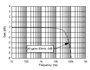
GUID-83617E96-1A29-4C2B-A85A-E17A105DCB76-low.gifFigure 9-4 Normalized Gain, All Variants
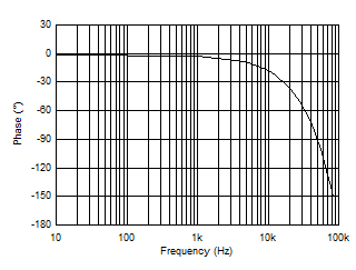
GUID-A218A869-706D-43BE-BBA1-0F5B3FBB9FCD-low.gifFigure 9-5 Normalized Phase, All Variants