SBOS835C May   2017  – October 2019 TMP464

PRODUCTION DATA.  

  1. Features
  2. Applications
  3. Description
    1.     Device Images
      1.      Typical Application Schematic
  4. Revision History
  5. Pin Configuration and Functions
    1.     Pin Functions
  6. Specifications
    1. 6.1 Absolute Maximum Ratings
    2. 6.2 ESD Ratings
    3. 6.3 Recommended Operating Conditions
    4. 6.4 Thermal Information
    5. 6.5 Electrical Characteristics
    6. 6.6 Two-Wire Timing Requirements
    7. 6.7 Typical Characteristics
  7. Detailed Description
    1. 7.1 Overview
    2. 7.2 Functional Block Diagram
    3. 7.3 Feature Description
      1. 7.3.1 Temperature Measurement Data
      2. 7.3.2 Series Resistance Cancellation
      3. 7.3.3 Differential Input Capacitance
      4. 7.3.4 Sensor Fault
      5. 7.3.5 THERM Functions
    4. 7.4 Device Functional Modes
      1. 7.4.1 Shutdown Mode (SD)
    5. 7.5 Programming
      1. 7.5.1 Serial Interface
        1. 7.5.1.1 Bus Overview
        2. 7.5.1.2 Bus Definitions
        3. 7.5.1.3 Serial Bus Address
        4. 7.5.1.4 Read and Write Operations
          1. 7.5.1.4.1 Single Register Reads
          2. 7.5.1.4.2 Block Register Reads
        5. 7.5.1.5 Timeout Function
        6. 7.5.1.6 High-Speed Mode
      2. 7.5.2 TMP464 Register Reset
      3. 7.5.3 Lock Register
    6. 7.6 Register Maps
      1. 7.6.1 Register Information
        1. 7.6.1.1  Pointer Register
        2. 7.6.1.2  Local and Remote Temperature Value Registers
        3. 7.6.1.3  Software Reset Register
        4. 7.6.1.4  THERM Status Register
        5. 7.6.1.5  THERM2 Status Register
        6. 7.6.1.6  Remote Channel Open Status Register
        7. 7.6.1.7  Configuration Register
        8. 7.6.1.8  η-Factor Correction Register
        9. 7.6.1.9  Remote Temperature Offset Register
        10. 7.6.1.10 THERM Hysteresis Register
        11. 7.6.1.11 Local and Remote THERM and THERM2 Limit Registers
        12. 7.6.1.12 Block Read - Auto Increment Pointer
        13. 7.6.1.13 Lock Register
        14. 7.6.1.14 Manufacturer and Device Identification Plus Revision Registers
  8. Application and Implementation
    1. 8.1 Application Information
    2. 8.2 Typical Application
      1. 8.2.1 Design Requirements
      2. 8.2.2 Detailed Design Procedure
      3. 8.2.3 Application Curve
  9. Power Supply Recommendations
  10. 10Layout
    1. 10.1 Layout Guidelines
    2. 10.2 Layout Example
  11. 11Device and Documentation Support
    1. 11.1 Receiving Notification of Documentation Updates
    2. 11.2 Community Resources
    3. 11.3 Trademarks
    4. 11.4 Electrostatic Discharge Caution
    5. 11.5 Glossary
  12. 12Mechanical, Packaging, and Orderable Information

Package Options

Mechanical Data (Package|Pins)
Thermal pad, mechanical data (Package|Pins)
Orderable Information

THERM Functions

Operation of the THERM (pin 10) and THERM2 (pin 11) interrupt pins are shown in Figure 12.

The hysteresis value is stored in the THERM Hysteresis register and applies to both the THERM and THERM2 interrupts.
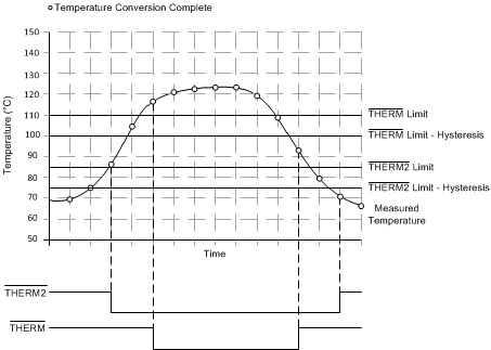
TMP464 ai_thermresp_slos877.gif
Figure 12. THERM and THERM2 Interrupt Operation