SBOS835C May 2017 – October 2019 TMP464
PRODUCTION DATA.
- 1 Features
- 2 Applications
- 3 Description
- 4 Revision History
- 5 Pin Configuration and Functions
- 6 Specifications
-
7 Detailed Description
- 7.1 Overview
- 7.2 Functional Block Diagram
- 7.3 Feature Description
- 7.4 Device Functional Modes
- 7.5 Programming
- 7.6
Register Maps
- 7.6.1
Register Information
- 7.6.1.1 Pointer Register
- 7.6.1.2 Local and Remote Temperature Value Registers
- 7.6.1.3 Software Reset Register
- 7.6.1.4 THERM Status Register
- 7.6.1.5 THERM2 Status Register
- 7.6.1.6 Remote Channel Open Status Register
- 7.6.1.7 Configuration Register
- 7.6.1.8 η-Factor Correction Register
- 7.6.1.9 Remote Temperature Offset Register
- 7.6.1.10 THERM Hysteresis Register
- 7.6.1.11 Local and Remote THERM and THERM2 Limit Registers
- 7.6.1.12 Block Read - Auto Increment Pointer
- 7.6.1.13 Lock Register
- 7.6.1.14 Manufacturer and Device Identification Plus Revision Registers
- 7.6.1
Register Information
- 8 Application and Implementation
- 9 Power Supply Recommendations
- 10Layout
- 11Device and Documentation Support
- 12Mechanical, Packaging, and Orderable Information
Package Options
Mechanical Data (Package|Pins)
- RGT|16
Thermal pad, mechanical data (Package|Pins)
- RGT|16
Orderable Information
8.2 Typical Application

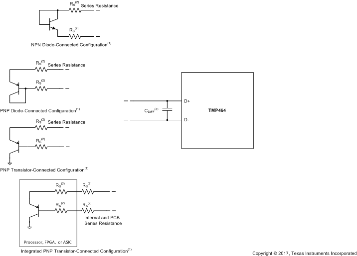
1. The diode-connected configuration provides better settling time. The transistor-connected configuration provides better series resistance cancellation. TI recommends a MMBT3904 or MMBT3906 transistor with an η-factor of 1.008.
2. RS (optional) is < 1 kΩ in most applications. RS is the combined series resistance connected externally to the D+, D– pins. RS selection depends on the application.
3. CDIFF (optional) is < 1000 pF in most applications. CDIFF selection depends on the application; see Figure 7.
4. Unused diode channels must be tied to D– .
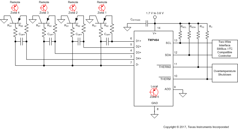
Figure 20. TMP464 Basic Connections Using a Discrete Remote Transistor  Figure 21. TMP464 Remote Transistor Configuration Options