SPRS377F September 2008 – June 2014 TMS320C6745 , TMS320C6747
PRODUCTION DATA.
- 1TMS320C6745, TMS320C6747 Fixed- and Floating-Point Digital Signal Processor
- 2Revision History
-
3Device Overview
- 3.1 Device Characteristics
- 3.2 Device Compatibility
- 3.3 DSP Subsystem
- 3.4 Memory Map Summary
- 3.5 Pin Assignments
- 3.6
Terminal Functions
- 3.6.1 Device Reset and JTAG
- 3.6.2 High-Frequency Oscillator and PLL
- 3.6.3 Real-Time Clock and 32-kHz Oscillator
- 3.6.4 External Memory Interface A (ASYNC, SDRAM)
- 3.6.5 External Memory Interface B (only SDRAM)
- 3.6.6 Serial Peripheral Interface Modules (SPI0, SPI1)
- 3.6.7 Enhanced Capture/Auxiliary PWM Modules (eCAP0, eCAP1, eCAP2)
- 3.6.8 Enhanced Pulse Width Modulators (eHRPWM0, eHRPWM1, eHRPWM2)
- 3.6.9 Enhanced Quadrature Encoder Pulse Module (eQEP)
- 3.6.10 Boot
- 3.6.11 Universal Asynchronous Receiver/Transmitters (UART0, UART1, UART2)
- 3.6.12 Inter-Integrated Circuit Modules (I2C0, I2C1)
- 3.6.13 Timers
- 3.6.14 Universal Host-Port Interface (UHPI)
- 3.6.15 Multichannel Audio Serial Ports (McASP0, McASP1, McASP2)
- 3.6.16 Universal Serial Bus Modules (USB0, USB1)
- 3.6.17 Ethernet Media Access Controller (EMAC)
- 3.6.18 Multimedia Card/Secure Digital (MMC/SD)
- 3.6.19 Liquid Crystal Display Controller (LCD)
- 3.6.20 General Purpose Input Output (GPIO)
- 3.6.21 Reserved and No Connect
- 3.6.22 Supply and Ground
- 3.6.23 Unused USB0 (USB2.0) and USB1 (USB1.1) Pin Configurations
- 4Device Configuration
-
5Device Operating Conditions
- 5.1 Absolute Maximum Ratings Over Operating Case Temperature Range (Unless Otherwise Noted)
- 5.2 Handling Ratings
- 5.3 Recommended Operating Conditions
- 5.4 Notes on Recommended Power-On Hours (POH)
- 5.5 Electrical Characteristics Over Recommended Ranges of Supply Voltage and Operating Case Temperature (Unless Otherwise Noted)
-
6Peripheral Information and Electrical Specifications
- 6.1 Parameter Information
- 6.2 Recommended Clock and Control Signal Transition Behavior
- 6.3 Power Supplies
- 6.4 Reset
- 6.5 Crystal Oscillator or External Clock Input
- 6.6 Clock PLLs
- 6.7 Interrupts
- 6.8 General-Purpose Input/Output (GPIO)
- 6.9 EDMA
- 6.10 External Memory Interface A (EMIFA)
- 6.11 External Memory Interface B (EMIFB)
- 6.12 Memory Protection Units
- 6.13 MMC / SD / SDIO (MMCSD)
- 6.14 Ethernet Media Access Controller (EMAC)
- 6.15 Management Data Input/Output (MDIO)
- 6.16 Multichannel Audio Serial Ports (McASP0, McASP1, and McASP2)
- 6.17
Serial Peripheral Interface Ports (SPI0, SPI1)
- 6.17.1 SPI Peripheral Registers Description(s)
- 6.17.2
SPI Electrical Data/Timing
- 6.17.2.1
Serial Peripheral Interface (SPI) Timing
- Table 6-54 General Timing Requirements for SPI0 Master Modes
- Table 6-55 General Timing Requirements for SPI0 Slave Modes
- Table 6-56 Additional SPI0 Master Timings, 4-Pin Enable Option
- Table 6-57 Additional SPI0 Master Timings, 4-Pin Chip Select Option
- Table 6-58 Additional SPI0 Master Timings, 5-Pin Option
- Table 6-59 Additional SPI0 Slave Timings, 4-Pin Enable Option
- Table 6-60 Additional SPI0 Slave Timings, 4-Pin Chip Select Option
- Table 6-61 Additional SPI0 Slave Timings, 5-Pin Option
- Table 6-62 General Timing Requirements for SPI1 Master Modes
- Table 6-63 General Timing Requirements for SPI1 Slave Modes
- Table 6-64 Additional SPI1 Master Timings, 4-Pin Enable Option
- Table 6-65 Additional SPI1 Master Timings, 4-Pin Chip Select Option
- Table 6-66 Additional SPI1 Master Timings, 5-Pin Option
- Table 6-67 Additional SPI1 Slave Timings, 4-Pin Enable Option
- Table 6-68 Additional SPI1 Slave Timings, 4-Pin Chip Select Option
- Table 6-69 Additional SPI1 Slave Timings, 5-Pin Option
- 6.17.2.1
Serial Peripheral Interface (SPI) Timing
- 6.18 Enhanced Capture (eCAP) Peripheral
- 6.19 Enhanced Quadrature Encoder (eQEP) Peripheral
- 6.20 Enhanced High-Resolution Pulse-Width Modulator (eHRPWM)
- 6.21 LCD Controller
- 6.22 Timers
- 6.23 Inter-Integrated Circuit Serial Ports (I2C0, I2C1)
- 6.24 Universal Asynchronous Receiver/Transmitter (UART)
- 6.25 USB1 Host Controller Registers (USB1.1 OHCI)
- 6.26 USB0 OTG (USB2.0 OTG)
- 6.27 Host-Port Interface (UHPI)
- 6.28 Power and Sleep Controller (PSC)
- 6.29 Programmable Real-Time Unit Subsystem (PRUSS)
- 6.30 Emulation Logic
- 6.31 IEEE 1149.1 JTAG
- 6.32 Real Time Clock (RTC)
- 7Device and Documentation Support
- 8Mechanical Packaging and Orderable Information
Package Options
Refer to the PDF data sheet for device specific package drawings
Mechanical Data (Package|Pins)
- ZKB|256
Thermal pad, mechanical data (Package|Pins)
Orderable Information
7 Mechanical Packaging and Orderable Information
This section describes the C6745/6747 orderable part numbers, packaging options, materials, thermal and mechanical parameters.
This section contains mechanical drawings for the ZKB Plastic Ball Grid Array package and the PTP PowerPAD™ plastic quad flat pack package. Additionally, for the PTP package a detailed drawing of the actual thermal pad dimensions as well as a recommended PCB footprint are provided.
7.1 Thermal Data for ZKB
The following table(s) show the thermal resistance characteristics for the PBGA–ZKB mechanical package.
Table 7-1 Thermal Resistance Characteristics (PBGA Package) [ZKB]
| No. | °C/W(1) | °C/W(2) | AIR FLOW (m/s)(3) | ||
|---|---|---|---|---|---|
| 1 | RΘJC | Junction-to-case | 12.8 | 13.5 | N/A |
| 2 | RΘJB | Junction-to-board | 15.1 | 19.7 | N/A |
| 3 | RΘJA | Junction-to-free air | 24.5 | 33.8 | 0.00 |
| 4 | RΘJMA | Junction-to-moving air | 21.9 | 30 | 0.50 |
| 5 | 21.1 | 28.7 | 1.00 | ||
| 6 | 20.4 | 27.4 | 2.00 | ||
| 7 | 19.6 | 26 | 4.00 | ||
| 8 | PsiJT | Junction-to-package top | 0.6 | 0.8 | 0.00 |
| 9 | 0.8 | 1 | 0.50 | ||
| 10 | 0.9 | 1.2 | 1.00 | ||
| 11 | 1.1 | 1.4 | 2.00 | ||
| 12 | 1.3 | 1.8 | 4.00 | ||
| 13 | PsiJB | Junction-to-board | 14.9 | 19.1 | 0.00 |
| 14 | 14.4 | 18.2 | 0.50 | ||
| 15 | 14.4 | 18 | 1.00 | ||
| 16 | 14.3 | 17.7 | 2.00 | ||
| 17 | 14.1 | 17.4 | 4.00 |
7.2 Thermal Data for PTP
The following table(s) show the thermal resistance characteristics for the PowerPAD™ PTP mechanical package.
Table 7-2 Thermal Resistance Characteristics (PowerPAD™ Package) [PTP]"
| No. | °C/W(1) | °C/W(2) | °C/W(3) | °C/W(4) | AIR FLOW (m/s)(5) | ||
|---|---|---|---|---|---|---|---|
| 1 | RΘJC | Junction-to-case | 7.8 | 9.4 | 8.6 | 10.1 | N/A |
| 2 | RΘJB | Junction-to-board | 6.2 | 9.9 | 7.1 | 10.6 | N/A |
| 3 | RΘJA | Junction-to-free air | 21.3 | 27.9 | 23.2 | 30.6 | 0.00 |
| 4 | RΘJMA | Junction-to-moving air | 14.3 | 20.2 | 22.6 | 0.50 | |
| 5 | 13.1 | 18.6 | 21.0 | 1.00 | |||
| 6 | 12.1 | 17.4 | 19.6 | 2.00 | |||
| 7 | 11.2 | 16.2 | 18.2 | 4.00 | |||
| 8 | PsiJT | Junction-to-package top | 0.5 | 0.7 | 0.8 | 0.00 | |
| 9 | 0.6 | 0.9 | 1.0 | 0.50 | |||
| 10 | 0.7 | 1.0 | 1.1 | 1.00 | |||
| 11 | 0.8 | 1.1 | 1.3 | 2.00 | |||
| 12 | 1.0 | 1.3 | 1.5 | 4.00 | |||
| 13 | PsiJB | Junction-to-board | 6.3 | 9.5 | 10.8 | 0.00 | |
| 14 | 5.9 | 8.8 | 9.9 | 0.50 | |||
| 15 | 5.9 | 8.7 | 9.8 | 1.00 | |||
| 16 | 5.8 | 8.6 | 9.7 | 2.00 | |||
| 17 | 5.8 | 8.5 | 9.6 | 4.00 |
7.3 Supplementary Information About the 176-pin PTP PowerPAD™ Package
This section highlights a few important details about the 176-pin PTP PowerPAD™ package. Texas Instruments' PowerPAD Thermally Enhanced Package Technical Brief (SLMA002) should be consulted when creating a PCB footprint for this device.
7.3.1 Standoff Height
As illustrated in Figure 7-1, the standoff height specification for this device (between 0.050 mm and 0.150 mm) is measured from the seating plane established by the three lowest package pins to the lowest point on the package body. Due to warpage, the lowest point on the package body is located in the center of the package at the exposed thermal pad.
Using this definition of standoff height provides the correct result for determining the correct solder paste thickness. According to TI's PowerPAD Thermally Enhanced Package Technical Brief (SLMA002), the recommended range of solder paste thickness for this package is between 0.152 mm and 0.178 mm.
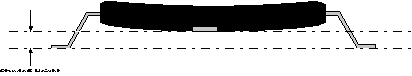 Figure 7-1 Standoff Height Measurement on 176-pin PTP Package
7.3.2 PowerPAD™ PCB Footprint
In general, for proper thermal performance, the thermal pad under the package body should be as large as possible. However, the soldermask opening for the PowerPAD™ should be sized to match the pad size on the 176-pin PTP package; as illustrated in Figure 7-2.
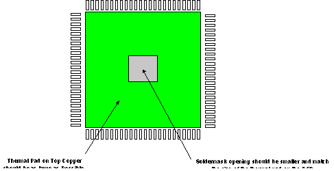 Figure 7-2 Soldermask Opening Should Match Size of DSP Thermal Pad
7.4 Packaging Information
The following packaging information and addendum reflect the most current data available for the designated device(s). This data is subject to change without notice and without revision of this document.