SPRSP25A June   2018  – July 2018 TMS320F28035-EP

PRODUCTION DATA.  

  1. 1Device Overview
    1. 1.1 Features
    2. 1.2 Applications
    3. 1.3 Description
    4. 1.4 Functional Block Diagram
  2. 2Revision History
  3. 3Terminal Configuration and Functions
    1. 3.1 Pin Diagram
    2. 3.2 Signal Descriptions
      1. Table 3-1 Signal Descriptions
  4. 4Specifications
    1. 4.1  Absolute Maximum Ratings
    2. 4.2  ESD Ratings
    3. 4.3  Power-On Hours (POH) Limits
    4. 4.4  Recommended Operating Conditions
    5. 4.5  Power Consumption Summary
      1. Table 4-1 TMS320F2803x Current Consumption at 60-MHz SYSCLKOUT
      2. 4.5.1      Reducing Current Consumption
      3. 4.5.2      Current Consumption Graphs (VREG Enabled)
    6. 4.6  Electrical Characteristics
    7. 4.7  Thermal Resistance Characteristics
    8. 4.8  Thermal Design Considerations
    9. 4.9  Emulator Connection Without Signal Buffering for the MCU
    10. 4.10 Parameter Information
      1. 4.10.1 Timing Parameter Symbology
      2. 4.10.2 General Notes on Timing Parameters
    11. 4.11 Test Load Circuit
    12. 4.12 Power Sequencing
      1. Table 4-4 Reset (XRS) Timing Requirements
      2. Table 4-5 Reset (XRS) Switching Characteristics
    13. 4.13 Clock Specifications
      1. 4.13.1 Device Clock Table
        1. Table 4-6 2803x Clock Table and Nomenclature (60-MHz Devices)
        2. Table 4-7 Device Clocking Requirements/Characteristics
        3. Table 4-8 Internal Zero-Pin Oscillator (INTOSC1/INTOSC2) Characteristics
      2. 4.13.2 Clock Requirements and Characteristics
        1. Table 4-9   XCLKIN Timing Requirements – PLL Enabled
        2. Table 4-10 XCLKIN Timing Requirements – PLL Disabled
        3. Table 4-11 XCLKOUT Switching Characteristics (PLL Bypassed or Enabled)
    14. 4.14 Flash Timing
      1. Table 4-12 Flash/OTP Endurance
      2. Table 4-13 Flash Parameters at 60-MHz SYSCLKOUT
      3. Table 4-14 Flash/OTP Access Timing
      4. Table 4-15 Flash Data Retention Duration
  5. 5Detailed Description
    1. 5.1 Overview
      1. 5.1.1  CPU
      2. 5.1.2  Control Law Accelerator (CLA)
      3. 5.1.3  Memory Bus (Harvard Bus Architecture)
      4. 5.1.4  Peripheral Bus
      5. 5.1.5  Real-Time JTAG and Analysis
      6. 5.1.6  Flash
      7. 5.1.7  M0, M1 SARAMs
      8. 5.1.8  L0 SARAM, and L1, L2, and L3 DPSARAMs
      9. 5.1.9  Boot ROM
        1. 5.1.9.1 Emulation Boot
        2. 5.1.9.2 GetMode
        3. 5.1.9.3 Peripheral Pins Used by the Bootloader
      10. 5.1.10 Security
      11. 5.1.11 Peripheral Interrupt Expansion (PIE) Block
      12. 5.1.12 External Interrupts (XINT1–XINT3)
      13. 5.1.13 Internal Zero Pin Oscillators, Oscillator, and PLL
      14. 5.1.14 Watchdog
      15. 5.1.15 Peripheral Clocking
      16. 5.1.16 Low-power Modes
      17. 5.1.17 Peripheral Frames 0, 1, 2, 3 (PFn)
      18. 5.1.18 General-Purpose Input/Output (GPIO) Multiplexer
      19. 5.1.19 32-Bit CPU-Timers (0, 1, 2)
      20. 5.1.20 Control Peripherals
      21. 5.1.21 Serial Port Peripherals
    2. 5.2 Memory Maps
    3. 5.3 Register Maps
    4. 5.4 Device Emulation Registers
    5. 5.5 VREG/BOR/POR
      1. 5.5.1 On-chip Voltage Regulator (VREG)
        1. 5.5.1.1 Using the On-chip VREG
        2. 5.5.1.2 Disabling the On-chip VREG
      2. 5.5.2 On-chip Power-On Reset (POR) and Brown-Out Reset (BOR) Circuit
    6. 5.6 System Control
      1. 5.6.1 Internal Zero Pin Oscillators
      2. 5.6.2 Crystal Oscillator Option
      3. 5.6.3 PLL-Based Clock Module
      4. 5.6.4 Loss of Input Clock (NMI Watchdog Function)
      5. 5.6.5 CPU-Watchdog Module
    7. 5.7 Low-Power Modes Block
    8. 5.8 Interrupts
      1. 5.8.1 External Interrupts
        1. 5.8.1.1 External Interrupt Electrical Data/Timing
          1. Table 5-20 External Interrupt Timing Requirements
          2. Table 5-21 External Interrupt Switching Characteristics
    9. 5.9 Peripherals
      1. 5.9.1  Control Law Accelerator (CLA) Overview
      2. 5.9.2  Analog Block
        1. 5.9.2.1 Analog-to-Digital Converter (ADC)
          1. 5.9.2.1.1 Features
          2. 5.9.2.1.2 ADC Start-of-Conversion Electrical Data/Timing
            1. Table 5-26 External ADC Start-of-Conversion Switching Characteristics
          3. 5.9.2.1.3 On-Chip Analog-to-Digital Converter (ADC) Electrical Data/Timing
            1. Table 5-27 ADC Electrical Characteristics
            2. Table 5-28 ADC Power Modes
            3. 5.9.2.1.3.1 Internal Temperature Sensor
              1. Table 5-29 Temperature Sensor Coefficient
            4. 5.9.2.1.3.2 ADC Power-Up Control Bit Timing
              1. Table 5-30 ADC Power-Up Delays
            5. 5.9.2.1.3.3 ADC Sequential and Simultaneous Timings
        2. 5.9.2.2 ADC MUX
        3. 5.9.2.3 Comparator Block
          1. 5.9.2.3.1 On-Chip Comparator/DAC Electrical Data/Timing
            1. Table 5-32 Electrical Characteristics of the Comparator/DAC
      3. 5.9.3  Detailed Descriptions
      4. 5.9.4  Serial Peripheral Interface (SPI) Module
        1. 5.9.4.1 SPI Master Mode Electrical Data/Timing
          1. Table 5-35 SPI Master Mode External Timing (Clock Phase = 0)
          2. Table 5-36 SPI Master Mode External Timing (Clock Phase = 1)
        2. 5.9.4.2 SPI Slave Mode Electrical Data/Timing
          1. Table 5-37 SPI Slave Mode External Timing (Clock Phase = 0)
          2. Table 5-38 SPI Slave Mode External Timing (Clock Phase = 1)
      5. 5.9.5  Serial Communications Interface (SCI) Module
      6. 5.9.6  Local Interconnect Network (LIN)
      7. 5.9.7  Enhanced Controller Area Network (eCAN) Module
      8. 5.9.8  Inter-Integrated Circuit (I2C)
        1. 5.9.8.1 I2C Electrical Data/Timing
          1. Table 5-44 I2C Timing Requirements
          2. Table 5-45 I2C Switching Characteristics
      9. 5.9.9  Enhanced PWM Modules (ePWM1/2/3/4/5/6/7)
        1. 5.9.9.1 ePWM Electrical Data/Timing
          1. Table 5-48 ePWM Timing Requirements
          2. Table 5-49 ePWM Switching Characteristics
        2. 5.9.9.2 Trip-Zone Input Timing
          1. Table 5-50 Trip-Zone Input Timing Requirements
      10. 5.9.10 High-Resolution PWM (HRPWM)
        1. 5.9.10.1 HRPWM Electrical Data/Timing
          1. Table 5-51 High-Resolution PWM Characteristics
      11. 5.9.11 Enhanced Capture Module (eCAP1)
        1. 5.9.11.1 eCAP Electrical Data/Timing
          1. Table 5-53 Enhanced Capture (eCAP) Timing Requirement
          2. Table 5-54 eCAP Switching Characteristics
      12. 5.9.12 High-Resolution Capture (HRCAP) Module
        1. 5.9.12.1 HRCAP Electrical Data/Timing
          1. Table 5-56 High-Resolution Capture (HRCAP) Timing Requirements
      13. 5.9.13 Enhanced Quadrature Encoder Pulse (eQEP)
        1. 5.9.13.1 eQEP Electrical Data/Timing
          1. Table 5-58 Enhanced Quadrature Encoder Pulse (eQEP) Timing Requirements
          2. Table 5-59 eQEP Switching Characteristics
      14. 5.9.14 JTAG Port
      15. 5.9.15 General-Purpose Input/Output (GPIO) MUX
        1. 5.9.15.1 GPIO Electrical Data/Timing
          1. 5.9.15.1.1 GPIO - Output Timing
            1. Table 5-63 General-Purpose Output Switching Characteristics
          2. 5.9.15.1.2 GPIO - Input Timing
            1. Table 5-64 General-Purpose Input Timing Requirements
          3. 5.9.15.1.3 Sampling Window Width for Input Signals
          4. 5.9.15.1.4 Low-Power Mode Wakeup Timing
            1. Table 5-65 IDLE Mode Timing Requirements
            2. Table 5-66 IDLE Mode Switching Characteristics
            3. Table 5-67 STANDBY Mode Timing Requirements
            4. Table 5-68 STANDBY Mode Switching Characteristics
            5. Table 5-69 HALT Mode Timing Requirements
            6. Table 5-70 HALT Mode Switching Characteristics
  6. 6Applications, Implementation, and Layout
    1. 6.1 TI Design or Reference Design
  7. 7Device and Documentation Support
    1. 7.1 Getting Started
    2. 7.2 Device and Development Support Tool Nomenclature
    3. 7.3 Tools and Software
    4. 7.4 Documentation Support
    5. 7.5 Community Resources
    6. 7.6 Trademarks
    7. 7.7 Electrostatic Discharge Caution
    8. 7.8 Glossary
  8. 8Mechanical, Packaging, and Orderable Information
    1. 8.1 Packaging Information

Package Options

Mechanical Data (Package|Pins)
Thermal pad, mechanical data (Package|Pins)
Orderable Information

Enhanced Quadrature Encoder Pulse (eQEP)

The device contains one enhanced quadrature encoder pulse (eQEP) module.

Table 5-57 eQEP Control and Status Registers

NAME eQEP1
ADDRESS
eQEP1
SIZE(x16)/
#SHADOW
REGISTER DESCRIPTION
QPOSCNT 0x6B00 2/0 eQEP Position Counter
QPOSINIT 0x6B02 2/0 eQEP Initialization Position Count
QPOSMAX 0x6B04 2/0 eQEP Maximum Position Count
QPOSCMP 0x6B06 2/1 eQEP Position-compare
QPOSILAT 0x6B08 2/0 eQEP Index Position Latch
QPOSSLAT 0x6B0A 2/0 eQEP Strobe Position Latch
QPOSLAT 0x6B0C 2/0 eQEP Position Latch
QUTMR 0x6B0E 2/0 eQEP Unit Timer
QUPRD 0x6B10 2/0 eQEP Unit Period Register
QWDTMR 0x6B12 1/0 eQEP Watchdog Timer
QWDPRD 0x6B13 1/0 eQEP Watchdog Period Register
QDECCTL 0x6B14 1/0 eQEP Decoder Control Register
QEPCTL 0x6B15 1/0 eQEP Control Register
QCAPCTL 0x6B16 1/0 eQEP Capture Control Register
QPOSCTL 0x6B17 1/0 eQEP Position-compare Control Register
QEINT 0x6B18 1/0 eQEP Interrupt Enable Register
QFLG 0x6B19 1/0 eQEP Interrupt Flag Register
QCLR 0x6B1A 1/0 eQEP Interrupt Clear Register
QFRC 0x6B1B 1/0 eQEP Interrupt Force Register
QEPSTS 0x6B1C 1/0 eQEP Status Register
QCTMR 0x6B1D 1/0 eQEP Capture Timer
QCPRD 0x6B1E 1/0 eQEP Capture Period Register
QCTMRLAT 0x6B1F 1/0 eQEP Capture Timer Latch
QCPRDLAT 0x6B20 1/0 eQEP Capture Period Latch
Reserved 0x6B21 – 0x6B3F 31/0

For more information on the eQEP, see the TMS320x2803x Piccolo Enhanced Quadrature Encoder Pulse (eQEP) Module Reference Guide.

Figure 5-40 shows the eQEP functional block diagram.
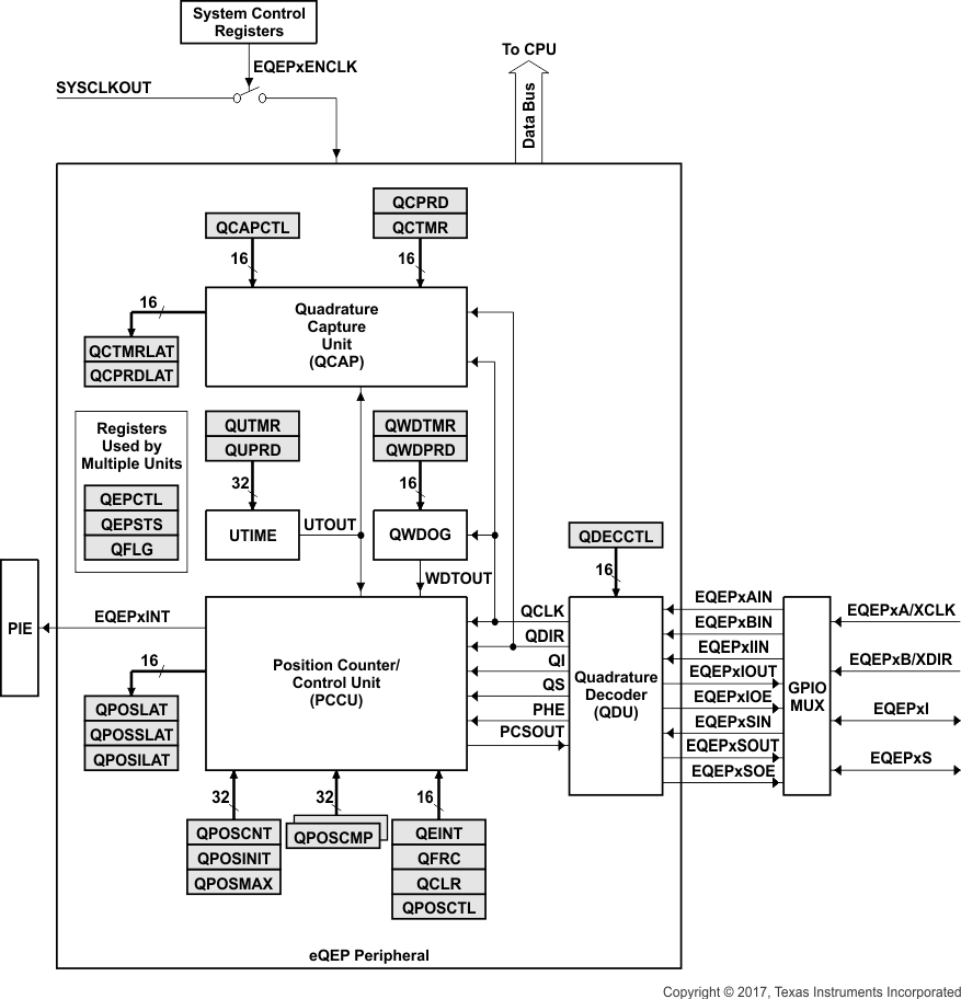
TMS320F28035-EP fbd_eqep_new_prs584.gifFigure 5-40 eQEP Functional Block Diagram