SPRS880P December   2013  – February 2024 TMS320F28374D , TMS320F28375D , TMS320F28376D , TMS320F28377D , TMS320F28377D-Q1 , TMS320F28378D , TMS320F28379D , TMS320F28379D-Q1

PRODUCTION DATA  

  1.   1
  2. Features
  3. Applications
  4. Description
    1. 3.1 Functional Block Diagram
  5. Device Comparison
    1. 4.1 Related Products
  6. Pin Configuration and Functions
    1. 5.1 Pin Diagrams
    2. 5.2 Signal Descriptions
      1. 5.2.1 Signal Descriptions
    3. 5.3 Pins With Internal Pullup and Pulldown
    4. 5.4 Pin Multiplexing
      1. 5.4.1 GPIO Muxed Pins
      2. 5.4.2 Input X-BAR
      3. 5.4.3 Output X-BAR and ePWM X-BAR
      4. 5.4.4 USB Pin Muxing
      5. 5.4.5 High-Speed SPI Pin Muxing
    5. 5.5 Connections for Unused Pins
  7. Specifications
    1. 6.1  Absolute Maximum Ratings
    2. 6.2  ESD Ratings – Commercial
    3. 6.3  ESD Ratings – Automotive
    4. 6.4  Recommended Operating Conditions
    5. 6.5  Power Consumption Summary
      1. 6.5.1 Device Current Consumption at 200-MHz SYSCLK
      2. 6.5.2 Current Consumption Graphs
      3. 6.5.3 Reducing Current Consumption
    6. 6.6  Electrical Characteristics
    7. 6.7  Thermal Resistance Characteristics
      1. 6.7.1 ZWT Package
      2. 6.7.2 PTP Package
      3. 6.7.3 PZP Package
    8. 6.8  Thermal Design Considerations
    9. 6.9  System
      1. 6.9.1  Power Sequencing
        1. 6.9.1.1 Signal Pin Requirements
        2. 6.9.1.2 VDDIO, VDDA, VDD3VFL, and VDDOSC Requirements
        3. 6.9.1.3 VDD Requirements
        4. 6.9.1.4 Supply Ramp Rate
          1. 6.9.1.4.1 Supply Ramp Rate
        5. 6.9.1.5 Supply Supervision
      2. 6.9.2  Reset Timing
        1. 6.9.2.1 Reset Sources
        2. 6.9.2.2 Reset Electrical Data and Timing
          1. 6.9.2.2.1 Reset ( XRS) Timing Requirements
          2. 6.9.2.2.2 Reset ( XRS) Switching Characteristics
      3. 6.9.3  Clock Specifications
        1. 6.9.3.1 Clock Sources
        2. 6.9.3.2 Clock Frequencies, Requirements, and Characteristics
          1. 6.9.3.2.1 Input Clock Frequency and Timing Requirements, PLL Lock Times
            1. 6.9.3.2.1.1 Input Clock Frequency
            2. 6.9.3.2.1.2 X1 Input Level Characteristics When Using an External Clock Source (Not a Crystal)
            3. 6.9.3.2.1.3 XTAL Oscillator Characteristics
            4. 6.9.3.2.1.4 X1 Timing Requirements
            5. 6.9.3.2.1.5 AUXCLKIN Timing Requirements
            6. 6.9.3.2.1.6 PLL Lock Times
          2. 6.9.3.2.2 Internal Clock Frequencies
            1. 6.9.3.2.2.1 Internal Clock Frequencies
          3. 6.9.3.2.3 Output Clock Frequency and Switching Characteristics
            1. 6.9.3.2.3.1 Output Clock Frequency
            2. 6.9.3.2.3.2 XCLKOUT Switching Characteristics (PLL Bypassed or Enabled)
        3. 6.9.3.3 Input Clocks and PLLs
        4. 6.9.3.4 XTAL Oscillator
          1. 6.9.3.4.1 Introduction
          2. 6.9.3.4.2 Overview
            1. 6.9.3.4.2.1 Electrical Oscillator
              1. 6.9.3.4.2.1.1 Modes of Operation
                1. 6.9.3.4.2.1.1.1 Crystal Mode of Operation
                2. 6.9.3.4.2.1.1.2 Single-Ended Mode of Operation
              2. 6.9.3.4.2.1.2 XTAL Output on XCLKOUT
            2. 6.9.3.4.2.2 Quartz Crystal
          3. 6.9.3.4.3 Functional Operation
            1. 6.9.3.4.3.1 ESR – Effective Series Resistance
            2. 6.9.3.4.3.2 Rneg – Negative Resistance
            3. 6.9.3.4.3.3 Start-up Time
            4. 6.9.3.4.3.4 DL – Drive Level
          4. 6.9.3.4.4 How to Choose a Crystal
          5. 6.9.3.4.5 Testing
          6. 6.9.3.4.6 Common Problems and Debug Tips
          7. 6.9.3.4.7 Crystal Oscillator Specifications
            1. 6.9.3.4.7.1 Crystal Oscillator Electrical Characteristics
            2. 6.9.3.4.7.2 Crystal Equivalent Series Resistance (ESR) Requirements
        5. 6.9.3.5 Internal Oscillators
          1. 6.9.3.5.1 Internal Oscillator Electrical Characteristics
      4. 6.9.4  Flash Parameters
        1. 6.9.4.1 Flash Parameters
      5. 6.9.5  RAM Specifications
      6. 6.9.6  ROM Specifications
      7. 6.9.7  Emulation/JTAG
        1. 6.9.7.1 JTAG Electrical Data and Timing
          1. 6.9.7.1.1 JTAG Timing Requirements
          2. 6.9.7.1.2 JTAG Switching Characteristics
      8. 6.9.8  GPIO Electrical Data and Timing
        1. 6.9.8.1 GPIO - Output Timing
          1. 6.9.8.1.1 General-Purpose Output Switching Characteristics
        2. 6.9.8.2 GPIO - Input Timing
          1. 6.9.8.2.1 General-Purpose Input Timing Requirements
        3. 6.9.8.3 Sampling Window Width for Input Signals
      9. 6.9.9  Interrupts
        1. 6.9.9.1 External Interrupt (XINT) Electrical Data and Timing
          1. 6.9.9.1.1 External Interrupt Timing Requirements
          2. 6.9.9.1.2 External Interrupt Switching Characteristics
      10. 6.9.10 Low-Power Modes
        1. 6.9.10.1 Clock-Gating Low-Power Modes
        2. 6.9.10.2 Power-Gating Low-Power Modes
        3. 6.9.10.3 Low-Power Mode Wakeup Timing
          1. 6.9.10.3.1 IDLE Mode Timing Requirements
          2. 6.9.10.3.2 IDLE Mode Switching Characteristics
          3. 6.9.10.3.3 STANDBY Mode Timing Requirements
          4. 6.9.10.3.4 STANDBY Mode Switching Characteristics
          5. 6.9.10.3.5 HALT Mode Timing Requirements
          6. 6.9.10.3.6 HALT Mode Switching Characteristics
          7. 6.9.10.3.7 HIBERNATE Mode Timing Requirements
          8. 6.9.10.3.8 HIBERNATE Mode Switching Characteristics
      11. 6.9.11 External Memory Interface (EMIF)
        1. 6.9.11.1 Asynchronous Memory Support
        2. 6.9.11.2 Synchronous DRAM Support
        3. 6.9.11.3 EMIF Electrical Data and Timing
          1. 6.9.11.3.1 Asynchronous RAM
            1. 6.9.11.3.1.1 EMIF Asynchronous Memory Timing Requirements
            2. 6.9.11.3.1.2 EMIF Asynchronous Memory Switching Characteristics
          2. 6.9.11.3.2 Synchronous RAM
            1. 6.9.11.3.2.1 EMIF Synchronous Memory Timing Requirements
            2. 6.9.11.3.2.2 EMIF Synchronous Memory Switching Characteristics
    10. 6.10 Analog Peripherals
      1. 6.10.1 Analog-to-Digital Converter (ADC)
        1. 6.10.1.1 ADC Configurability
          1. 6.10.1.1.1 Signal Mode
        2. 6.10.1.2 ADC Electrical Data and Timing
          1. 6.10.1.2.1 ADC Operating Conditions (16-Bit Differential Mode)
          2. 6.10.1.2.2 ADC Characteristics (16-Bit Differential Mode)
          3. 6.10.1.2.3 ADC Operating Conditions (12-Bit Single-Ended Mode)
          4. 6.10.1.2.4 ADC Characteristics (12-Bit Single-Ended Mode)
          5. 6.10.1.2.5 ADCEXTSOC Timing Requirements
          6. 6.10.1.2.6 ADC Input Models
            1. 6.10.1.2.6.1 Differential Input Model Parameters
            2. 6.10.1.2.6.2 Single-Ended Input Model Parameters
          7. 6.10.1.2.7 ADC Timing Diagrams
            1. 6.10.1.2.7.1 ADC Timings in 12-Bit Mode (SYSCLK Cycles)
            2. 6.10.1.2.7.2 ADC Timings in 16-Bit Mode
        3. 6.10.1.3 Temperature Sensor Electrical Data and Timing
          1. 6.10.1.3.1 Temperature Sensor Electrical Characteristics
      2. 6.10.2 Comparator Subsystem (CMPSS)
        1. 6.10.2.1 CMPSS Electrical Data and Timing
          1. 6.10.2.1.1 Comparator Electrical Characteristics
          2. 6.10.2.1.2 CMPSS DAC Static Electrical Characteristics
      3. 6.10.3 Buffered Digital-to-Analog Converter (DAC)
        1. 6.10.3.1 Buffered DAC Electrical Data and Timing
          1. 6.10.3.1.1 Buffered DAC Electrical Characteristics
        2. 6.10.3.2 CMPSS DAC Dynamic Error
    11. 6.11 Control Peripherals
      1. 6.11.1 Enhanced Capture (eCAP)
        1. 6.11.1.1 eCAP Electrical Data and Timing
          1. 6.11.1.1.1 eCAP Timing Requirement
          2. 6.11.1.1.2 eCAP Switching Characteristics
      2. 6.11.2 Enhanced Pulse Width Modulator (ePWM)
        1. 6.11.2.1 Control Peripherals Synchronization
        2. 6.11.2.2 ePWM Electrical Data and Timing
          1. 6.11.2.2.1 ePWM Timing Requirements
          2. 6.11.2.2.2 ePWM Switching Characteristics
          3. 6.11.2.2.3 Trip-Zone Input Timing
            1. 6.11.2.2.3.1 Trip-Zone Input Timing Requirements
        3. 6.11.2.3 External ADC Start-of-Conversion Electrical Data and Timing
          1. 6.11.2.3.1 External ADC Start-of-Conversion Switching Characteristics
      3. 6.11.3 Enhanced Quadrature Encoder Pulse (eQEP)
        1. 6.11.3.1 eQEP Electrical Data and Timing
          1. 6.11.3.1.1 eQEP Timing Requirements
          2. 6.11.3.1.2 eQEP Switching Characteristics
      4. 6.11.4 High-Resolution Pulse Width Modulator (HRPWM)
        1. 6.11.4.1 HRPWM Electrical Data and Timing
          1. 6.11.4.1.1 High-Resolution PWM Timing Requirements
          2. 6.11.4.1.2 High-Resolution PWM Characteristics
      5. 6.11.5 Sigma-Delta Filter Module (SDFM)
        1. 6.11.5.1 SDFM Electrical Data and Timing (Using ASYNC)
          1. 6.11.5.1.1 SDFM Timing Requirements When Using Asynchronous GPIO (ASYNC) Option
        2. 6.11.5.2 SDFM Electrical Data and Timing (Using 3-Sample GPIO Input Qualification)
          1. 6.11.5.2.1 SDFM Timing Requirements When Using GPIO Input Qualification (3-Sample Window) Option
    12. 6.12 Communications Peripherals
      1. 6.12.1 Controller Area Network (CAN)
      2. 6.12.2 Inter-Integrated Circuit (I2C)
        1. 6.12.2.1 I2C Electrical Data and Timing
          1. 6.12.2.1.1 I2C Timing Requirements
          2. 6.12.2.1.2 I2C Switching Characteristics
          3. 6.12.2.1.3 I2C Timing Diagram
      3. 6.12.3 Multichannel Buffered Serial Port (McBSP)
        1. 6.12.3.1 McBSP Electrical Data and Timing
          1. 6.12.3.1.1 McBSP Transmit and Receive Timing
            1. 6.12.3.1.1.1 McBSP Timing Requirements
            2. 6.12.3.1.1.2 McBSP Switching Characteristics
          2. 6.12.3.1.2 McBSP as SPI Master or Slave Timing
            1. 6.12.3.1.2.1 McBSP as SPI Master Timing Requirements
            2. 6.12.3.1.2.2 McBSP as SPI Master Switching Characteristics
            3. 6.12.3.1.2.3 McBSP as SPI Slave Timing Requirements
            4. 6.12.3.1.2.4 McBSP as SPI Slave Switching Characteristics
      4. 6.12.4 Serial Communications Interface (SCI)
      5. 6.12.5 Serial Peripheral Interface (SPI)
        1. 6.12.5.1 SPI Electrical Data and Timing
          1. 6.12.5.1.1 SPI Master Mode Timings
            1. 6.12.5.1.1.1 SPI Master Mode Timing Requirements
            2. 6.12.5.1.1.2 SPI Master Mode Switching Characteristics (Clock Phase = 0)
            3. 6.12.5.1.1.3 SPI Master Mode Switching Characteristics (Clock Phase = 1)
          2. 6.12.5.1.2 SPI Slave Mode Timings
            1. 6.12.5.1.2.1 SPI Slave Mode Timing Requirements
            2. 6.12.5.1.2.2 SPI Slave Mode Switching Characteristics
      6. 6.12.6 Universal Serial Bus (USB) Controller
        1. 6.12.6.1 USB Electrical Data and Timing
          1. 6.12.6.1.1 USB Input Ports DP and DM Timing Requirements
          2. 6.12.6.1.2 USB Output Ports DP and DM Switching Characteristics
      7. 6.12.7 Universal Parallel Port (uPP) Interface
        1. 6.12.7.1 uPP Electrical Data and Timing
          1. 6.12.7.1.1 uPP Timing Requirements
          2. 6.12.7.1.2 uPP Switching Characteristics
  8. Detailed Description
    1. 7.1  Overview
    2. 7.2  Functional Block Diagram
    3. 7.3  Memory
      1. 7.3.1 C28x Memory Map
      2. 7.3.2 Flash Memory Map
      3. 7.3.3 EMIF Chip Select Memory Map
      4. 7.3.4 Peripheral Registers Memory Map
      5. 7.3.5 Memory Types
        1. 7.3.5.1 Dedicated RAM (Mx and Dx RAM)
        2. 7.3.5.2 Local Shared RAM (LSx RAM)
        3. 7.3.5.3 Global Shared RAM (GSx RAM)
        4. 7.3.5.4 CPU Message RAM (CPU MSGRAM)
        5. 7.3.5.5 CLA Message RAM (CLA MSGRAM)
    4. 7.4  Identification
    5. 7.5  Bus Architecture – Peripheral Connectivity
    6. 7.6  C28x Processor
      1. 7.6.1 Floating-Point Unit
      2. 7.6.2 Trigonometric Math Unit
      3. 7.6.3 Viterbi, Complex Math, and CRC Unit II (VCU-II)
    7. 7.7  Control Law Accelerator
    8. 7.8  Direct Memory Access
    9. 7.9  Interprocessor Communication Module
    10. 7.10 Boot ROM and Peripheral Booting
      1. 7.10.1 EMU Boot or Emulation Boot
      2. 7.10.2 WAIT Boot Mode
      3. 7.10.3 Get Mode
      4. 7.10.4 Peripheral Pins Used by Bootloaders
    11. 7.11 Dual Code Security Module
    12. 7.12 Timers
    13. 7.13 Nonmaskable Interrupt With Watchdog Timer (NMIWD)
    14. 7.14 Watchdog
    15. 7.15 Configurable Logic Block (CLB)
    16. 7.16 Functional Safety
  9. Applications, Implementation, and Layout
    1. 8.1 Application and Implementation
    2. 8.2 Key Device Features
    3. 8.3 Application Information
      1. 8.3.1 Typical Application
        1. 8.3.1.1 Servo Drive Control Module
          1. 8.3.1.1.1 System Block Diagram
          2. 8.3.1.1.2 Servo Drive Control Module Resources
        2. 8.3.1.2 Solar Micro Inverter
          1. 8.3.1.2.1 System Block Diagram
          2. 8.3.1.2.2 Solar Micro Inverter Resources
        3. 8.3.1.3 On-Board Charger (OBC)
          1. 8.3.1.3.1 System Block Diagram
          2. 8.3.1.3.2 OBC Resources
        4. 8.3.1.4 EV Charging Station Power Module
          1. 8.3.1.4.1 System Block Diagram
          2. 8.3.1.4.2 EV Charging Station Power Module Resources
        5. 8.3.1.5 High-Voltage Traction Inverter
          1. 8.3.1.5.1 System Block Diagram
          2. 8.3.1.5.2 High-Voltage Traction Inverter Resources
  10. Device and Documentation Support
    1. 9.1 Device and Development Support Tool Nomenclature
    2. 9.2 Markings
    3. 9.3 Tools and Software
    4. 9.4 Documentation Support
    5. 9.5 Support Resources
    6. 9.6 Trademarks
    7. 9.7 Electrostatic Discharge Caution
    8. 9.8 Glossary
  11. 10Revision History
  12. 11Mechanical, Packaging, and Orderable Information
    1. 11.1 Packaging Information

Package Options

Refer to the PDF data sheet for device specific package drawings

Mechanical Data (Package|Pins)
  • PTP|176
Thermal pad, mechanical data (Package|Pins)
Orderable Information

Direct Memory Access

Each CPU has its own 6-channel DMA module. The DMA module provides a hardware method of transferring data between peripherals and/or memory without intervention from the CPU, thereby freeing up bandwidth for other system functions. Additionally, the DMA has the capability to orthogonally rearrange the data as it is transferred as well as “ping-pong” data between buffers. These features are useful for structuring data into blocks for optimal CPU processing.

The DMA module is an event-based machine, meaning it requires a peripheral or software trigger to start a DMA transfer. Although it can be made into a periodic time-driven machine by configuring a timer as the interrupt trigger source, there is no mechanism within the module itself to start memory transfers periodically. The interrupt trigger source for each of the six DMA channels can be configured separately and each channel contains its own independent PIE interrupt to let the CPU know when a DMA transfer has either started or completed. Five of the six channels are exactly the same, while Channel 1 has the ability to be configured at a higher priority than the others.

DMA features include:

  • Six channels with independent PIE interrupts
  • Peripheral interrupt trigger sources
    • ADC interrupts and EVT signals
    • Multichannel buffered serial port transmit and receive
    • External interrupts
    • CPU timers
    • EPWMxSOC signals
    • SPIx transmit and receive
    • SDFM
    • Software trigger
  • Data sources and destinations:
    • GSx RAM
    • CPU message RAM (IPC RAM)
    • ADC result registers
    • ePWMx
    • SPI
    • McBSP
    • EMIF
  • Word Size: 16-bit or 32-bit (SPI and McBSP limited to 16-bit)
  • Throughput: four cycles/word (without arbitration)

Figure 7-3 shows a device-level block diagram of the DMA.
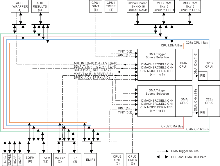
GUID-9516A097-069F-4EE1-86EE-8CFD86736847-low.gif Figure 7-3 DMA Block Diagram