SLAS997B March 2014 – January 2015 TPA6166A2
PRODUCTION DATA.
- 1 Features
- 2 Applications
- 3 Description
- 4 Revision History
- 5 Pin Configuration and Functions
- 6 Specifications
-
7 Detailed Description
- 7.1 Overview
- 7.2 Functional Block Diagram
- 7.3 Feature Description
- 7.4 Device Functional Modes
- 7.5
Register Maps
- 7.5.1 Register Functional Overview
- 7.5.2 Initialization
- 7.5.3 Typical Use Case Modes
- 7.5.4 Recommended Software Flow Chart
- 7.5.5 Register Map Summary
- 7.5.6
Detailed Register Descriptions
- 7.5.6.1 Register 0x00: Config and Device Status Register 1
- 7.5.6.2 Register 0x01: Config and Device Status Register 2
- 7.5.6.3 Register 0x02: Config and Device Status Register 2
- 7.5.6.4 Register 0x03: Reserved Register
- 7.5.6.5 Register 0x04: Interrupt Mask Register 1
- 7.5.6.6 Register 0x05: Interrupt Mask Register 2
- 7.5.6.7 Register 0x06: Reserved Register
- 7.5.6.8 Register 0x07: Headphone Volume Register 1
- 7.5.6.9 Register 0x08: Headphone Volume Control Register 2
- 7.5.6.10 Register 0x09: Microphone Bias Control Register
- 7.5.6.11 Register 0x0a: Reserved
- 7.5.6.12 Register 0x0b: Revision ID Register
- 7.5.6.13 Register 0x0c: Reserved Register
- 7.5.6.14 Registers 0x0d to 0x10: Reserved Registers
- 7.5.6.15 Register 0x11: Reserved
- 7.5.6.16 Register 0x12: Reserved
- 7.5.6.17 Register 0x13: Reserved
- 7.5.6.18 Register 0x14: Reserved Register
- 7.5.6.19 Register 0x15: Keyscan Debounce Register
- 7.5.6.20 Register 0x16: Keyscan Delay Register
- 7.5.6.21 Register 0x17: Passive Multi Button Keyscan Data Register
- 7.5.6.22 Register 0x18: Jack Detect Test Hardware Settings
- 7.5.6.23 Register 0x19:State Register
- 7.5.6.24 Register 0x1a: Jack Detect Test Hardware Settings
- 7.5.6.25 Registers 0x1b: Reserved
- 7.5.6.26 Register 0x1c: Clock Control
- 7.5.6.27 Register 0x1d: Enable Register 1
- 7.5.6.28 Register 0x1e: Enable Register 2
- 7.5.6.29 Register 0x1F: Reserved
- 7.5.6.30 Register 0x66: Clock Flex Register
- 7.5.6.31 Register 0x6F: Clock Set Register
- 8 Application and Implementation
- 9 Power Supply Recommendations
- 10Layout
- 11Device and Documentation Support
- 12Mechanical, Packaging, and Orderable Information
Package Options
Mechanical Data (Package|Pins)
- YFF|25
Thermal pad, mechanical data (Package|Pins)
Orderable Information
8 Application and Implementation
NOTE
Information in the following applications sections is not part of the TI component specification, and TI does not warrant its accuracy or completeness. TI’s customers are responsible for determining suitability of components for their purposes. Customers should validate and test their design implementation to confirm system functionality.
8.1 Application Information
This section describes a typical application of TPA6166A2 with a standard audio jack with battery voltage level supply. The circuit detects what kind of device is plugged into the jack and delivers excellent audio quality.
8.2 Typical Application
Figure 32 shows a typical application circuit for the TPA6166A2 with a 5-terminal audio jack. Accessory Detection describes all the accessory jack configurations the TPA6166A2 automatically detects.
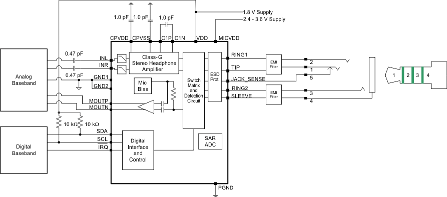 Figure 32. Typical Application Circuit
8.2.1 Design Requirements
Table 7. Design Parameters
| DESIGN PARAMETERS | VALUE |
|---|---|
| VDD Supply voltage | 1.7 V to 1.9 V |
| MICVDD Microphone supply voltage | 2.4 V to 3.6 V |
8.2.2 Detailed Design Procedure
8.2.2.1 Charge Pump Capacitors
The CPVDD and CPVSS capacitor must be at least equal in value to the flying capacitor to allow maximum charge transfer. Use low ESR (example: < 20 mΩ at 1.3 MHz) ceramic capacitors to maximize charge pump efficiency. X5R-type capacitors or better are required for best performance. Typical values are 1 µF to 2.2 µF for the charge pump capacitors.
Charge pump capacitors should be able to handle up to 2 V during normal operation. During IEC ESD strike on jack terminals, voltage on these capacitors can go as high as 12 V for 30 to 40 ns. Capacitors rated for 6.3 V or higher can typically handle such voltages for short durations without getting damaged.
8.2.2.2 Audio Input ac Coupling Capacitors
Input coupling capacitors block any dc bias from the audio source and ensure maximum dynamic range. Input coupling capacitors also minimize TPA6166A2 turnon pop to an inaudible level. The input capacitors are in series with TPA6166A2 internal input resistors, creating a high-pass filter. Equation 2 calculates the high-pass filter corner frequency. The TPA6166A2 typical input impedance, RIN, is 20 kΩ.
For a given high-pass cutoff frequency, the minimum input coupling capacitor is:
Example: Select input coupling capacitor values to achieve a 20 Hz high-pass corner frequency. Equation 3 shows the input coupling capacitors must be at least 0.4 μF. Choose a 0.47-μF standard value capacitor for each TPA6166A2 input. Use X5R-type or better capacitors for best performance.
8.2.2.3 Suggested Output EMI Filter
To prevent noise getting radiated from headphone, EMI filters are often included on terminals connected to the Jack. Figure 33 illustrates typical connection diagram of EMI filter implemented using ‘pi’ configuration.
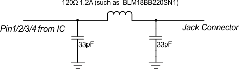 Figure 33. EMI Filter
High-frequency impedance of RF beads in range of 100 MHz can impact IEC ESD performance on TPA6166A2 jack outputs (LOUT, PIN2_ROUT, PIN3, and PIN4). Higher impedances change the waveform during IEC strike to make it wider, which subjects internal circuit to stress for longer duration. Use RF beads which are equal to or less than 22-Ω impedance at 100 MHz.
8.2.3 Application Curve
The high quality and low distortion of the TPA6166A2 mic preamplifier is shown in Figure 34.
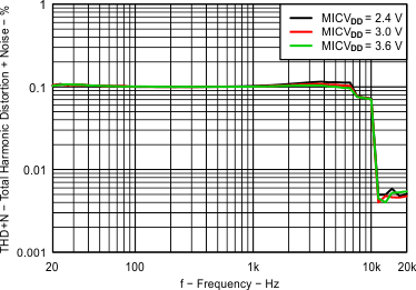 Figure 34. Mic Preamplifier Total Harmonic Distortion + Noise vs Frequency