SLAS997B March 2014 – January 2015 TPA6166A2
PRODUCTION DATA.
- 1 Features
- 2 Applications
- 3 Description
- 4 Revision History
- 5 Pin Configuration and Functions
- 6 Specifications
-
7 Detailed Description
- 7.1 Overview
- 7.2 Functional Block Diagram
- 7.3 Feature Description
- 7.4 Device Functional Modes
- 7.5
Register Maps
- 7.5.1 Register Functional Overview
- 7.5.2 Initialization
- 7.5.3 Typical Use Case Modes
- 7.5.4 Recommended Software Flow Chart
- 7.5.5 Register Map Summary
- 7.5.6
Detailed Register Descriptions
- 7.5.6.1 Register 0x00: Config and Device Status Register 1
- 7.5.6.2 Register 0x01: Config and Device Status Register 2
- 7.5.6.3 Register 0x02: Config and Device Status Register 2
- 7.5.6.4 Register 0x03: Reserved Register
- 7.5.6.5 Register 0x04: Interrupt Mask Register 1
- 7.5.6.6 Register 0x05: Interrupt Mask Register 2
- 7.5.6.7 Register 0x06: Reserved Register
- 7.5.6.8 Register 0x07: Headphone Volume Register 1
- 7.5.6.9 Register 0x08: Headphone Volume Control Register 2
- 7.5.6.10 Register 0x09: Microphone Bias Control Register
- 7.5.6.11 Register 0x0a: Reserved
- 7.5.6.12 Register 0x0b: Revision ID Register
- 7.5.6.13 Register 0x0c: Reserved Register
- 7.5.6.14 Registers 0x0d to 0x10: Reserved Registers
- 7.5.6.15 Register 0x11: Reserved
- 7.5.6.16 Register 0x12: Reserved
- 7.5.6.17 Register 0x13: Reserved
- 7.5.6.18 Register 0x14: Reserved Register
- 7.5.6.19 Register 0x15: Keyscan Debounce Register
- 7.5.6.20 Register 0x16: Keyscan Delay Register
- 7.5.6.21 Register 0x17: Passive Multi Button Keyscan Data Register
- 7.5.6.22 Register 0x18: Jack Detect Test Hardware Settings
- 7.5.6.23 Register 0x19:State Register
- 7.5.6.24 Register 0x1a: Jack Detect Test Hardware Settings
- 7.5.6.25 Registers 0x1b: Reserved
- 7.5.6.26 Register 0x1c: Clock Control
- 7.5.6.27 Register 0x1d: Enable Register 1
- 7.5.6.28 Register 0x1e: Enable Register 2
- 7.5.6.29 Register 0x1F: Reserved
- 7.5.6.30 Register 0x66: Clock Flex Register
- 7.5.6.31 Register 0x6F: Clock Set Register
- 8 Application and Implementation
- 9 Power Supply Recommendations
- 10Layout
- 11Device and Documentation Support
- 12Mechanical, Packaging, and Orderable Information
Package Options
Mechanical Data (Package|Pins)
- YFF|25
Thermal pad, mechanical data (Package|Pins)
Orderable Information
10 Layout
10.1 Layout Guidelines
The ground terminal must be connected to the ground plane as close as possible to the TPA6166A2, to minimize any inductance in the path. Place the decoupling capacitor as close as possible to the supply terminal, minimizing trace length (and thus the inductance) on the decoupling capacitor connection to ground.
Because INL and INR are single-ended inputs, take care to minimize noise on INL and INR with respect to TPA6166A2 ground. This is best achieved by using then same ground plane for the signal source and the TPA6166A2 with a minimum inductance between them.
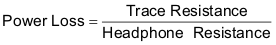
The accessory-detection algorithm requires trace capacitance to be minimized between TPA6166A2 and the jack. Depending upon headphone impedance, trace resistance between TPA6166A2 and the jack impacts power delivered to load. If trace resistance is much smaller than headphone impedance, power loss is given by Equation 4. Trace resistance should be minimized based on acceptable power loss.
To minimize crosstalk, trace resistance on RING2 (terminal 3) and SLEEVE (terminal 4) should be minimized. This can be achieved by placing TPA6166A2 close to the jack. For cases where trace resistance is not small, crosstalk is given by Equation 5. In such scenarios, best balance can be achieved by increasing trace width of SLEEVE. RING2 has no constraint on maximum capacitance, and its trace width can be maximized to achieve desired crosstalk performance.

10.2 Layout Example
10.2.1 Pad Sizing
When determining the pad size for the WCSP terminals, use nonsolder mask defined (NSMD) land. With this method, the solder mask opening is made larger than the desired land area, and the opening size is defined by the copper pad width. Figure 35 and Table 8 show the appropriate diameters for a WCSP layout.
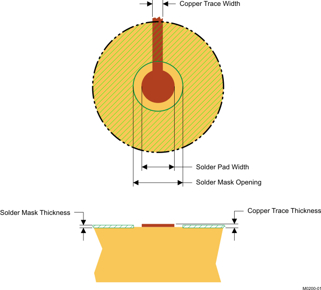 Figure 35. Land Pattern Dimensions
Table 8. Land Pattern Dimensions (1)(2)(3)(4)
| SOLDER PAD DEFINITION | COPPER PAD | SOLDER MASK(5) OPENING | COPPER THICKNESS | STENCIL(6)(7)
OPENING |
STENCIL THICKNESS |
|---|---|---|---|---|---|
| Nonsolder mask defined (NSMD) | 230 μm | 310 μm | 1 oz. max. (32 μm) | 275 μm × 275 μm sq. (rounded corners) | 100 μm thick |
Table 9. Package Dimensions
| D | E |
|---|---|
| Max. = 2470 µm | Max. = 2470 µm |
| Typ. = 2440 µm | Typ. = 2440 µm |
| Min. = 2410 µm | Min. = 2410 µm |