SLAS997B March 2014 – January 2015 TPA6166A2
PRODUCTION DATA.
- 1 Features
- 2 Applications
- 3 Description
- 4 Revision History
- 5 Pin Configuration and Functions
- 6 Specifications
-
7 Detailed Description
- 7.1 Overview
- 7.2 Functional Block Diagram
- 7.3 Feature Description
- 7.4 Device Functional Modes
- 7.5
Register Maps
- 7.5.1 Register Functional Overview
- 7.5.2 Initialization
- 7.5.3 Typical Use Case Modes
- 7.5.4 Recommended Software Flow Chart
- 7.5.5 Register Map Summary
- 7.5.6
Detailed Register Descriptions
- 7.5.6.1 Register 0x00: Config and Device Status Register 1
- 7.5.6.2 Register 0x01: Config and Device Status Register 2
- 7.5.6.3 Register 0x02: Config and Device Status Register 2
- 7.5.6.4 Register 0x03: Reserved Register
- 7.5.6.5 Register 0x04: Interrupt Mask Register 1
- 7.5.6.6 Register 0x05: Interrupt Mask Register 2
- 7.5.6.7 Register 0x06: Reserved Register
- 7.5.6.8 Register 0x07: Headphone Volume Register 1
- 7.5.6.9 Register 0x08: Headphone Volume Control Register 2
- 7.5.6.10 Register 0x09: Microphone Bias Control Register
- 7.5.6.11 Register 0x0a: Reserved
- 7.5.6.12 Register 0x0b: Revision ID Register
- 7.5.6.13 Register 0x0c: Reserved Register
- 7.5.6.14 Registers 0x0d to 0x10: Reserved Registers
- 7.5.6.15 Register 0x11: Reserved
- 7.5.6.16 Register 0x12: Reserved
- 7.5.6.17 Register 0x13: Reserved
- 7.5.6.18 Register 0x14: Reserved Register
- 7.5.6.19 Register 0x15: Keyscan Debounce Register
- 7.5.6.20 Register 0x16: Keyscan Delay Register
- 7.5.6.21 Register 0x17: Passive Multi Button Keyscan Data Register
- 7.5.6.22 Register 0x18: Jack Detect Test Hardware Settings
- 7.5.6.23 Register 0x19:State Register
- 7.5.6.24 Register 0x1a: Jack Detect Test Hardware Settings
- 7.5.6.25 Registers 0x1b: Reserved
- 7.5.6.26 Register 0x1c: Clock Control
- 7.5.6.27 Register 0x1d: Enable Register 1
- 7.5.6.28 Register 0x1e: Enable Register 2
- 7.5.6.29 Register 0x1F: Reserved
- 7.5.6.30 Register 0x66: Clock Flex Register
- 7.5.6.31 Register 0x6F: Clock Set Register
- 8 Application and Implementation
- 9 Power Supply Recommendations
- 10Layout
- 11Device and Documentation Support
- 12Mechanical, Packaging, and Orderable Information
Package Options
Mechanical Data (Package|Pins)
- YFF|25
Thermal pad, mechanical data (Package|Pins)
Orderable Information
7 Detailed Description
7.1 Overview
The TPA6166A2 is a small device that serves a large number of complex functions in a portable audio device. It identifies an accessory plugged into the jack, and configures the internal subsystems to take full advantage of its capabilities.
- Headphone-jack accessory detection and identification
- Switch matrix
- Class-G ground-centered stereo headphone amplifier
- Mic preamplifier and bias
- SAR ADC for various analog sense functions
- ESD protection
- Convenient I2C host interface
7.2 Functional Block Diagram
7.3 Feature Description
7.3.1 I2C Interface
The TPA6166A2 I2C address is 0x40 (7-bit).
The I2C bus employs two signals, SDA (data) and SCL (clock), to communicate between integrated circuits in a system. The bus transfers data serially, one bit at a time. The most significant bit (MSB) is transferred first for the 8-bit address and data bytes. In addition, each byte transferred on the bus is acknowledged by the receiving device with an acknowledge bit. Each transfer operation begins with the master device driving a start condition on the bus and ends with the master device driving a stop condition on the bus. The bus uses transitions on the data terminal (SDA) while the clock is at logic high to indicate start and stop conditions. A high-to-low transition on SDA indicates a start and a low-to-high transition indicates a stop. Normal data-bit transitions must occur within the low time of the clock period.
Figure 22 shows a typical sequence. The master generates the 7-bit slave address and the read/write (R/W) bit to open communication with another device, and then waits for an acknowledge condition. The TPA6166A2 holds SDA low during the acknowledge clock period to indicate acknowledgment. When acknowledgment occurs, the master transmits the next byte of the sequence. Each device is addressed by a unique 7-bit slave address plus R/W bit (1 byte). All compatible devices share the same signals via a bidirectional bus using a wired-AND connection.
An external pullup resistor must be used for the SDA and SCL signals to set the logic high level for the bus. When the bus level is 3.3 V, use pullup resistors between 1 kΩ and 2 kΩ.
There is no limit on the number of bytes that can be transmitted between start and stop conditions. When the last word transfers, the master generates a stop condition to release the bus. A generic data transfer sequence is shown in Figure 22.
 Figure 22. Typical I2C Sequence
7.3.1.1 Single and Multiple Byte Transfers
The serial control interface supports both single-byte and multiple byte read/write operations for all registers. During multiple-byte read operations, the TPA6166A2 responds with data, 1 byte at a time, starting at the register assigned, as long as the master device continues to respond with acknowledgments.
The TPA6166A2 supports sequential I2C addressing. For write transactions, if a register is issued followed by data for that register and all the remaining registers that follow, a sequential I2C write transaction has occurred. For I2C sequential write transactions, the register issued then serves as the starting point, and the amount of data subsequently transmitted, before a stop or start is transmitted, determines the number of registers written.
7.3.1.2 Single-Byte Write
As Figure 23 shows, a single-byte data write transfer begins with the master device transmitting a start condition followed by the I2C device address and the read/write bit. The read/write bit determines the direction of the data transfer. For a write data transfer, the read/write bit must be set to 0. After receiving the correct I2C device address and the read/write bit, the TPA6166A2 responds with an acknowledge bit. Next, the master transmits the register byte corresponding to the TPA6166A2 internal memory address being accessed. After receiving the register byte, the TPA6166A2 again responds with an acknowledge bit. Next, the master device transmits the data byte to be written to the memory address being accessed. After receiving the register byte, the TPA6166A2 again responds with an acknowledge bit. Finally, the master device transmits a stop condition to complete the single-byte data write transfer.
 Figure 23. Single-Byte Write Transfer
7.3.1.3 Multiple-Byte Write and Incremental Multiple-Byte Write
A multiple-byte data write transfer is identical to a single-byte data write transfer except that multiple data bytes are transmitted by the master device to the TPA6166A2 as shown in Figure 24. After receiving each data byte, the TPA6166A2 responds with an acknowledge bit.
 Figure 24. Multiple-Byte Write Transfer
7.3.1.4 Single-Byte Read
As Figure 25 shows, a single-byte data read transfer begins with the master device transmitting a start condition followed by the I2C device address and the read/write bit. For the data read transfer, both a write followed by a read are actually executed. Initially, a write is executed to transfer the address byte of the internal memory address to be read. As a result, the read/write bit is set to a 0.
After receiving the TPA6166A2 address and the read/write bit, the TPA6166A2 responds with an acknowledge bit. The master then sends the internal memory address byte, after which the TPA6166A2 issues an acknowledge bit. The master device transmits another start condition followed by the TPA6166A2 address and the read/write bit again. This time the read/write bit is set to 1, indicating a read transfer. Next, the TPA6166A2 transmits the data byte from the memory address being read. After receiving the data byte, the master device transmits a not-acknowledge followed by a stop condition to complete the single-byte data read transfer.
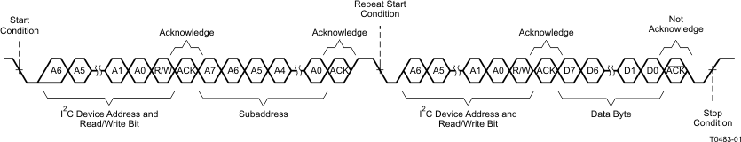 Figure 25. Single-Byte Read Transfer
7.3.1.5 Multiple-Byte Read
A multiple-byte data read transfer is identical to a single-byte data read transfer except that multiple data bytes are transmitted by the TPA6166A2 to the master device as shown in Figure 26. With the exception of the last data byte, the master device responds with an acknowledge bit after receiving each data byte.
 Figure 26. Multiple-Byte Read Transfer
7.3.2 Accessory Detection
The TPA6166A2 has an advanced accessory jack detection circuitry which determines insertion, removal, as well as type detection of accessories with a 3.5-mm headset jack. The jack and its internal connections are shown in Figure 27.
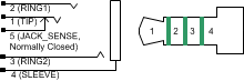 Figure 27. Connecting to a 3.5-mm Headset Jack
When the insertion of a jack is detected, the accessory type detection algorithm runs until two consecutive type detections produce the same result. In general, the type detection algorithm is not run again after this point of time. Hence, on-the-fly change of accessory type is not detected. The following accessories can be detected. Table 6 has specific detection details.
- Stereo Headset (HP with mic)
- Line Out Audio Cable
- Mono Headset
- Stereo Headphone
- Line Out Audio Cable
The limits of detection are shown in Table 1.
Table 1. Limits of Detection
| PARAMETER | SYMBOL | MIN | MAX | UNIT |
|---|---|---|---|---|
| Cable Shield Capacitance | CCABLE | 150 | 500 | pF |
| Headphone Load Resistance | RHP | 8 | 700/1500* | Ω |
| Audio Line Load Resistance | RLINE | 10 | 50 | kΩ |
| Microphone Load Resistance | RMIC | 1.5 | 20 | kΩ |
| Open/Float | 200K || 70 pF | 10 G || 5 pF | kΩ |
As a result of accessory detection, appropriate blocks are automatically turned on ensuring lower possible power consumption. When accessory is removed, all blocks are turned off ensuring ultra low power. The TPA6166A2 achieves 22.7 µW when no accessory is inserted.
7.3.3 Audio Playback Channel
The TPA6166A2 includes stereo audio channel with integrated low pass filter and class-G headphone amplifier. Figure 28 shows the block diagram for the Audio Channel. The channel includes volume control block. The volume level can be varied from +6 dB to –42 dB in 1-dB steps, in addition to a mute bit, independently for each channel. The volume level of both channels can also be changed simultaneously by the master volume control, which can be achieved by setting Register 0x07, Bit 7 (L=R) to 1. Gain changes are implemented with a soft-stepping algorithm, which only changes the actual volume by one step in every 3.25 ms, either up or down, until the desired volume is reached.
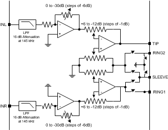 Figure 28. Audio Playback Channel
Because of soft-stepping, the system does not know when the audio channel has been actually muted. This may be important if the system wishes to mute the channel before making a significant change. To help with this situation, the device provides a flag back to the system through a read-only register bit that alerts the system when the part has completed the soft-stepping and the actual volume has reached the desired volume level. Soft-stepping feature can be disabled by setting Register 0x1E, Bit 5 (VSEN) to 1.
The TPA6166A2 integrates switches on RING2 (terminal 3) and SLEEVE (terminal 4) to ground. Based on accessory detection result, either RING2 or SLEEVE is selected as accessory ground, and appropriate switch is turned on. As switches have finite resistance, it can give rise to crosstalk between left and right channel. The TPA6166A2 integrates ground loop rejection circuitry, which reduces crosstalk to a great extent.
The left channel audio output can be routed to TIP. For right channel, audio output is routed to RING1.
7.3.3.1 Class-G Headphone Amplifier
Class-G is a linear amplifier using a modulating supply voltage. A high-efficiency step-down converter regulates the headphone amplifier supply voltage. The headphone amplifier supply voltage increases as the audio output voltage increases. This prevents signal clipping and distortion. The headphone amplifier supply voltage decreases during softer audio periods, reducing battery current and improving overall efficiency. The class-G amplifier has more than twice the efficiency of an equivalent class-AB amplifier. This increases battery life during audio playback.
Figure 29 shows the block diagram for the class-G headphone amplifier. The class-G control examines the amplifier output voltage and determines the optimum headphone supply voltage. CPVDD and CPVSS voltages increase fast enough to avoid any output clipping or distortion. The class-G control operates automatically and does not require programming.
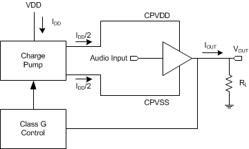 Figure 29. Class-G Headphone Block Diagram
7.3.3.1.1 Headphone Charge Pump
The TPA6166A2 includes a high-efficiency step-down charge pump and an inverting charge pump to generate power supplies for the headphone amplifier. These charge pumps use a common flying capacitor, thus minimizing components. The step-down charge pump regulates CPVDD; the inverting charge pump regulates CPVSS. These are designed to only drive the TPA6166A2 headphone amplifier. Do not use CPVDD or CPVSS as a voltage supply to drive an external device.
7.3.3.2 Out-of-Band and Input RF Noise Rejection
When using amplifiers with CODECs and DACs, sometimes there is an increase in the output noise floor from the audio amplifier. This occurs when the output out-of-band noise of the CODEC/DAC folds back into the audio frequency due to the limited gain bandwidth product of the audio amplifier. Single-ended RF noise can also fold back into the audio band thus degrading the audio signal even further.
The TPA6166A2 has a built-in low-pass filter to reduce CODEC/DAC out-of-band noise and RF noise, that could fold back into the audio frequency.
7.3.4 Mic Channel
The TPA6166A2 includes microphone preamplifier with selectable gain of 12 dB and 24 dB. The device uses architecture, which removes requirement of external AC coupling capacitor by integrating it inside. The TPA6166A2 also includes Mic-bias with integrated bias resistor. A mic bias voltage can be programmed to 2.0 V or 2.6 V. Mic-bias resistor can be programmed to 2.2 kΩ, 2.6 kΩ, 3.0 kΩ or bypass. Based on accessory detection result, either RING2 (terminal 3 of jack) or SLEEVE (terminal 4 of jack) is selected as Mic input, and appropriate switch is turned on. Figure 30 shows the block diagram for the Mic Channel. Note that Bias resistor bypass mode, accessory detection, removal detection, and mic amp will not function.
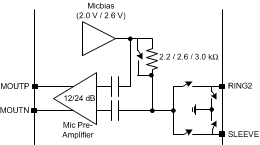 Figure 30. Mic Channel
7.3.5 Button Press Detection
The TPA6166A2 supports button press detection of different types:
- Single button press/release: When pressed, this typically creates an equivalent resistance of 1 Ω between RING2 and SLEEVE.
- Passive button press/release: When pressed, this creates an equivalent resistance between RING2 and SLEEVE. The TPA6166A2 reports press and release event along with resistance value (KEYDATA_DIV and KEYDATA in Register 0x17).
The impedance seen by the ADC is calculated using the following data
- Bias voltage
- Bias resistor
- Parallel impedance of the switch pressed and the microphone capsule impedance
The button press detection is done in a two-stage process. The device remains in a low power mode until a comparator is tripped. The comparator threshold is set to <1500Ω. Upon detection, the ADC is started to calculate the impedance pressed.
NOTE
The ADC will support impedances up to 375 Ω. Higher values are supported, but are much more susceptible to capacitance in the mic capsule, and could potentially provide erronious readings. At 375 Ω, Mic Capsule capacitances supported can be up to 50 nF.
For more details on configuring the device for Button Press Detection, see Button Detection.
7.4 Device Functional Modes
7.4.1 I2C Options
The TPA6166A2 I2C address is 0x40 (7-bit).
7.4.2 System in Shutdown Mode
Shutdown mode enables lowest power consumption from device. During this mode, accessory insertion, removal and type detection are not supported, but as soon as system comes out of shutdown, detection will work fine.
This mode can be programmed by programming /SHDN, register 0x1D (bit-7) to 0 For coming out of shutdown, /SHDN bit should be set to 1.
This will also rerun accessory detection algorithm.
7.4.3 System in Sleep Mode
This mode is enabled by programming SLEEP, register 0x1D (bit-6) to 1. During this mode, accessory insertion, removal, type and single-button press/release detection are supported.
7.4.3.1 Accessory Not Inserted
When the device is in AUTO mode (register 0x1E, bit 1-0 = 01), the device automatically configures itself in lowest possible power mode.
If accessory was previously inserted and is then removed, interrupt gets generated. Upon interrupt following sequence can be used to determine accessory removal and take appropriate action:
- Read control registers 0x00 to 0x02
- If JKIN, register 0x00, bit-7 = 0, then infer that accessory has been removed. Program SLEEP, register 0x1D, bit-6 = 1.
7.4.3.2 Accessory Inserted
When the device is in AUTO (register 0x1E, bit 1-0 = 01) and SLEEP (register 0x1D, bit-6 = 1) mode, the device automatically configures itself to minimize power consumption. For example: the mic preamplifier and headphone amplifiers are turned off, but removal and button-press detection continue to operate.
If the accessory was previously not inserted and is then inserted, interrupt gets generated. Upon interrupt following sequence can be used to determine accessory insertion and take appropriate action:
- Read control registers 0x00 to 0x02
- If JKIN, register 0x00, bit 7 = 1, then infer that accessory has been inserted.
- Read control register 0x19 to determine type of accessory
When the system wakes up and programs the device out of SLEEP mode, appropriate blocks will automatically turn on based on the type of accessory. System can also use accessory type to configure different routings (example: mix left and right channel for mono headset) and signal swing (depending on whether it is headphone or line-out load).
If the system was previously not in sleep mode and enters sleep mode, the following sequence should be followed to avoid pop noise on the headphone output:
- Enable interrupt due to volume slewing. This can be done by programming register 0x04, bit-5 (IVOL) = 1.
- If register 0x07, bit-7 (L=R) is 1, then program register 0x1E, bits 7-6 (left and right headphone control) = 00 and bits 1-0 (AUTO) = 00. Wait for interrupt due to volume slewing complete (VOL, register 0x00, bit-5).
- If register 0x07, bit-7 (L=R) is 0, then execute following steps:
- If register 0x1E, bit-7=1, then program register 0x1E, bit-7 = 0 and bits 1-0 = 00. Wait for interrupt due to volume slewing complete (VOL, register 0x00, bit-5)
- If register 0x1E, bit-6=1, then program register 0x1E, bit-6 = 0 and bits 1-0 = 00. Wait for interrupt due to volume slewing complete (VOL, register 0x00, bit-5).
- Program device in sleep mode (register 0x1D, bit-6, SLEEP = 1).
- Program device back in Auto mode (register 0x1E, bits 1-0, AUTO = 01.
7.4.3.3 Button Detection During Sleep Mode
During Sleep mode, single-button press/release detection is supported. Remaining buttons of passive multi-button headset (resistance of button higher than 0 Ω) are also detected as single button (resistance ≈ 0 Ω). For a button press, the system can use this event to wake up the system, and then program the device (details in Button Detection) to detect the second button press correctly.
Upon interrupt, the following sequence needs to be followed for button detection:
- Read control registers 0x00 to 0x02
- If MCSW, register 0x00, bit 1 = 1, then infer that button has been pressed/released. As long as button is pressed, MCSW continues to remain set.
7.4.4 System in Wake-Up Mode
This mode is enabled by programming SLEEP, register 0x1D (bit-6) to 0. During this mode, accessory insertion, removal, type, single button press/release and passive multi-button detection are supported.
7.4.4.1 Accessory Not Inserted
When the device is in AUTO mode (register 0x1E, bit 1-0 = 01), the device automatically configures itself in lowest possible power mode.
If accessory was previously inserted and is then removed, interrupt gets generated. Upon interrupt following sequence can be used to determine accessory removal and take appropriate action:
- Read control registers 0x00 to 0x02
- If JKIN, register 0x00, bit 7 = 0, then infer that accessory has been removed. Program SLEEP, register 0x1D, bit-6 = 1.
If a voice call is in progress, the system can use removal information to change from headset to handset mode. If audio is playing, the system can use the removal information to route audio to the speaker amplifier.
7.4.4.2 Accessory Inserted
When the device is in AUTO mode (register 0x1E, bit 1-0 = 01), the device automatically configures itself to turn on appropriate blocks. For example: for mono, only left headphone amp is turned on, whereas for stereo both left and right headphone amps are turned on).
If accessory was previously not inserted and is then inserted, an interrupt is generated. Upon an interrupt, the following sequence can be used to determine that an accessory insertion has occurred and take appropriate action:
- Read control registers 0x00 to 0x02
- If JKIN, register 0x00, bit-7 = 1, then infer that accessory has been inserted.
- Read control register 0x19 (bit 6-0, STATE) to determine type of accessory. Program SLEEP, register 0x1D, bit-6 = 0 (if audio is playing or in voice call).
If a voice call is in progress, the system can use the insertion information to change from handset to headset mode. If audio is playing on speaker, the system can use the insertion information to route audio to headset (accessory).
Accessory type detection can be used to configure different routings (example: for mono headset, mix left and right channel and route it on INL of the TPA6166A2) and signal swing (depending on headphone or line-out load).
7.4.4.3 Audio Not Playing or Not in Voice Call
During this mode, lowest power option is to program the device in SLEEP mode (register 0x1D, bit 6 = 1). This will power down mic preamplifier and headphone amplifiers. If audio starts playing or a voice call starts, SLEEP can be programmed to 0. To minimize pop and clock, headphone amplifiers go through power up sequencing where it first powers up in MUTE and then soft step volume to set gain with slew rate of 3.25 ms/dB. Volume slewing can be disabled by programming register 0x1E, bit-5 to 1.
7.4.4.4 High Impedance Line Out Load
The TPA6166A2 detects 50-kΩ max impedance as a line-level output. A value above 50 kΩ is treated as float and the corresponding amplifier is kept powered down. If higher value line-out load must be supported, the following sequence can be used, when accessory insertion is detected:
- Register 0x19 (bit 6-0, STATE) value is already available immediately after insertion detection (to determine type of accessory). Check if STATE have one of following values
- 0x1B
- 0x1C
- 0x1F
- If value matches one of the above, the following register writes should be done
- Register 0x19 (bits 7-0) = 0x1A
- Register 0x19 (bits 7-0) = 0x9A
The preceding sequence will power up both left and right headphone amplifiers. After this step, the device will again go into automatic mode, where blocks will be powered up and down based on detection result.
7.4.4.5 Button Detection
If only single-button detection is required, following sequence can be used when interrupt is generated:
- Read control registers 0x00 to 0x02
- If MCSW, register 0x00, bit 1 = 1, then infer that button has been pressed (PRESS, register 0x01, bit-1 = 1) or released (PRESS, register 0x01, bit-1 = 0)
If both single-button and passive multi-button detection are required, the following sequence can be used:
- As soon as the device is in wake-up mode (SLEEP = 0), following register writes should be done
- Register 0x1C (bit-7) = 1
- Register 0x66 (bits 7-0) = 0xF1
- Register 0x6F (bits 7-0) = 0x01
- Register 0x66 (bits 7-0) = 0x00
- Upon interrupt, following sequence can be used:
- Read control registers 0x00 to 0x02
- If MCSW (register 0x00, bit-1) = 1, then infer that single-button has been pressed (PRESS, register 0x01, bit-1 = 1) or released (PRESS, register 0x01, bit-1 = 0).
- If MCSW = 0 and KEY (register 0x01, bit-2) = 1, then infer that passive multi-button has been pressed (PRESS, register 0x01, bit-1 = 1) or released (PRESS, register 0x01, bit-1 = 0).
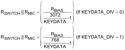
- If passive multi-button press is detected, value of button resistance can be known by reading register 0x17 (KEYDATA_DIV and KEYDATA). Equation for resistance calculation is shown in description of control register 0x17
- When device needs to be taken to Sleep or Shutdown mode or accessory removal gets detected, the following additional registers should be programmed to minimize power consumption
- Register 0x1C (bit-7) = 0
- Register 0x66 (bits 7-0) = 0xF1
- Register 0x6F (bits 7-0) = 0x00
- Register 0x66 (bits 7-0) = 0x00
7.5 Register Maps
7.5.1 Register Functional Overview
The TPA6166A2 when configured in fully automated mode (bits 1-0, register 0x1E set to 01) automatically enables and disables relevant blocks (headphone, mic preamplifier, mic bias, and so forth) based on result of accessory detection.
Table 2. Register Descriptions for Software Developers
| Registers | Read/Write | Function |
|---|---|---|
| 0x00, 0x01, 0x02 | R | Configuration and device status registers. These registers are used to report the makeup of the inserted jack as well as report when a microphone switch has been pressed or the jack has been removed. The TPA6166A2 uses the status registers and IRQ to report the status of various device functions. The status registers bits are set when their respective event occurs and cleared upon reading the register. Device status can be determined either by polling the registers or configuring the IRQ to go low when specific events occur and then reading these registers on IRQ. |
| 0x04, 0x05 | R/W | Interrupt mask registers. These registers determine which bits in the status registers (0x00 – 0x02) will trigger IRQ to go low. Once IRQ goes low, it becomes high when status register responsible for IRQ generation gets read. |
| 0x07, 0x08 | R/W | Headphone volume setting registers. These registers independently control and report the gain of the left and right headphone amplifiers. There is an option to have right channel gain track left channel gain setting. This can be done by setting bit 7 in control register 0x07. |
| 0x09 | R/W | Microphone bias and preamplifier setting register. This register is used to program different settings related to microphone preamplifier and microphone bias. |
| 0x0B | R | Revision ID register |
| 0x15, 0x16 | R/W | Passive multi-button debounce and delay settings. Debounce helps in filtering any unwanted noise/glitches in system which can cause wrong button detection. The delay register sets the time-out that the mic button press is masked from the system. At the end of the delay time, the TPA6166A2 checks to see if accessory is still present. If accessory is not present, then it does not generate interrupt corresponding to button press. This prevents accessory removal from being detected as a button press (due to RING2 and SLEEVE getting shorted during removal). |
| 0x17 | R | Passive multi-button data register. For resistance calculations, refer to control register description in data sheet |
| 0x19 | R/W | State Register. Indicates type of accessory (headset with/without mic, headphone, line-out, no accessory inserted, and so forth). If AUTO mode (default) is turned on, relevant blocks are automatically turned on/off based on type of accessory. |
| 0x18, 0x1A | R/W | Accessory detection test hardware settings. Provides fine-tuning for accessory detection algorithm. |
| 0x1C | R/W | Clock control for passive multi button. Needed to be configured along with few other registers for passive multi-button to work. Refer to control register description in data sheet for details. |
| 0x1D, 0x1E | R/W | Enable settings register. This contains all of the bits that control the separate functional blocks. The system can either directly control these bits, or it can allow device to automatically configure itself and report which blocks are enabled. When the AUTO bits (B1-B0) are set to 01 or 10, this register is read only. The block enable bits do not need to be set to detect accessory insertion/removal. |
| 0x03, 0x06, 0x0A, 0x0C, 0x0D – 0x14, 0x1B, 0x1F | R/W | Reserved. Always write recommended values to these registers. |
7.5.2 Initialization
7.5.2.1 Reserved Registers
Always program values based on Table 3 (registers in bold must be programmed).
Table 3. Initialization of Reserved Registers
| Register Address | Value (Hex) | Comments |
|---|---|---|
| 0x03 | 00 | Same as default |
| 0x06 | 00 | Same as default |
| 0x0A | 00 | Same as default |
| 0x0C | 1C | Same as default |
| 0x0D | 00 | Same as default |
| 0x0E | 00 | Same as default |
| 0x0F | 00 | Same as default |
| 0x10 | 00 | Same as default |
| 0x11 | 00 | Same as default |
| 0x12 | 01 | Default is 00 |
| 0x13 | 45 | Default is 00 |
| 0x14 | 00 | Same as default |
| 01B | 00 | Default is not defined |
| 0x1F | 00 | Same as default |
7.5.2.2 Fixed Registers
Values for these registers will likely remain same all the time. Table below have recommended settings for registers. Based on system requirement, it is possible that slightly different values need to be programmed.
Table 4. Typically Fixed Registers
| Register Address | Value (Binary) | Comments |
|---|---|---|
| 0x04 | 1100 0010 | Same as default |
| 0x05 | 0000 0100 | Same as default |
| 0x09 | B7B6B5B4B3B200 | Bits 1-0 must be programmed to 00. Bits 7-2 values based on system need (Example: 0100 01 for 24-dB mic preamplifier gain, 2.2-kΩ bias resistor and 2.6-V bias voltage ) |
| 0x15 | 1111 1111 | Debounce time of ~64 ms. If this causes too much delay for button press detection, then lower value can be considered. |
| 0x16 | 1111 1111 | Debounce time of ~256 ms. If this causes too much delay for button press detection, then lower value can be considered. |
| 0x18 | 1100 0000 | Same as default |
| 0x1A | 1001 0101 | Same as default |
7.5.2.3 Other Registers
Values for these registers will likely be changed by system on-the-fly depending on mode of operation
Table 5. Commonly Used Registers
| Register Address | Value (Binary) | Comments |
|---|---|---|
| 0x1E | 0001 10001 | TI recommends programming this register first before anything else in this table |
| 0x07 | 0000 0100 | Bits 6-0 values based on system need (Example: 011 1001 for 0dB gain). These bits can be changed on-the-fly for controlling volume. |
| 0x08 | 1B6B5B4B3B2B1B0 | Bits 6-0 are don’t care if bit 7 of register 0x1E is set to 1 |
| 0x1C | 0000 0000 | Bit-7 will likely change based on mode, if passive multi-button needs to be supported. |
| 0x1D | 1100 0000 |
7.5.3 Typical Use Case Modes
After initialization, registers described in Section will need to be programmed during different modes. In addition, the following registers will be used for checking status, configuration and measurement data:
- 0x00
- 0x01
- 0x02
- 0x17
- 0x19
Upon interrupt, the system host should read registers 0x00, 0x01 and 0x02 to determine the interrupt source and respond appropriately.
- System In Shutdown Mode
- System In Sleep Mode
- Accessory Not Inserted
- Accessory Inserted
- Button Detection During Sleep Mode
- System In Wake-Up Mode
- Accessory Not Inserted
- Accessory Inserted
- Audio Not Playing Or Not In Voice Call
- High Impedance Line-Out Load
- Button Detection
- Accessory Insertion/Removal Detection Without Using Jack_sense
- Scheme 1
- Scheme 2
- Special Headset Detection
7.5.4 Recommended Software Flow Chart
The flow chart in Figure 31 gives a conceptual view of how software can be organized for different modes.
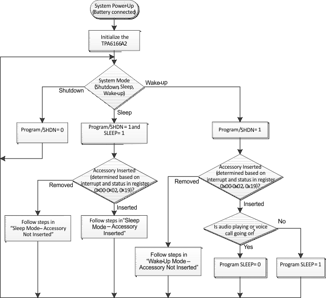 Figure 31. Recommended Software Flow Chart
7.5.5 Register Map Summary
The TPA6166A2 I2C address is 0x40 (7-bit). See I2C Interface for more details.
| REGISTER | READ / WRITE |
DEFAULT | FUNCTION | |
|---|---|---|---|---|
| DEC | HEX | |||
| 0 | 0x00 | R | 0x00 | Configuration and Device Status Register 1 |
| 1 | 0x01 | R | 0x00 | Configuration and Device Status Register 2 |
| 2 | 0x02 | R | 0x00 | Configuration and Device Status Register 3 |
| 3 | 0x03 | R | 0x00 | Reserved. Always write 0x00 |
| 4 | 0x04 | R/W | 0x00 | Interrupt Mask Register 1 |
| 5 | 0x05 | R/W | 0x00 | Interrupt Mask Register 2 |
| 6 | 0x06 | R/W | 0x00 | Reserved. Always write 0x00 |
| 7 | 0x07 | R/W | 0xC0 | Headphone Volume Control Register 1 |
| 8 | 0x08 | R/W | 0x40 | Headphone Volume Control Register 2 |
| 9 | 0x09 | R/W | 0x03 | Microphone Bias Control Register |
| 10 | 0x0A | R | 0x00 | Reserved |
| 11 | 0x0B | R | 0x30 | Revision ID Register |
| 12 | 0x0C | R/W | 0x1C | Reserved. |
| 13 | 0x0D | R/W | 0x00 | Reserved. Always write 0x00 |
| 14 | 0x0E | R/W | 0x00 | Reserved. Always write 0x00 |
| 15 | 0x0F | R/W | 0x00 | Reserved. Always write 0x00 |
| 16 | 0x10 | R/W | 0x00 | Reserved. Always write 0x00 |
| 17 | 0x11 | R/W | 0x00 | Reserved. Always write 0x00 |
| 18 | 0x12 | R/W | 0x00 | Reserved. Always write 0x01 |
| 19 | 0x13 | R/W | 0x00 | Reserved. Always write 0x45 |
| 20 | 0x14 | R | 0x00 | Reserved. |
| 21 | 0x15 | R/W | 0x00 | Keyscan Debounce Register |
| 22 | 0x16 | R/W | 0x00 | Keyscan Delay Register |
| 23 | 0x17 | R | 0x00 | Passive Multi Button Keyscan Data Register |
| 24 | 0x18 | R/W | 0x00 | Jack Detect Test Hardware Settings |
| 25 | 0x19 | R/W | 0x80 | State Register |
| 26 | 0x1A | R/W | 0x15 | Jack Detect Test Hardware Settings |
| 27 | 0x1B | R | Reserved | |
| 28 | 0x1C | R/W | 0x01 | Clock control. Initiialize it to 0x00 |
| 29 | 0x1D | R/W | 0x00 | Enable Register 1 |
| 30 | 0x1E | R/W | 0x01 | Enable Register 2 |
| 31 | 0x1F | R | 0x00 | Reserved |
Registers 0x00, 0x01, and 0x02 are used to report the makeup of the inserted jack as well as report when a microphone switch has been pressed or the jack has been removed. The TPA6166A2 uses the status registers and IRQ to report the status of various device functions. The status registers bits are set when their respective event occurs and cleared upon reading the register. Device status can be determined either by polling the registers or configuring the IRQ to go low when specific events occur. Registers 0x04 and 0x05 determine which bits in the status register will trigger IRQ to go low. Once IRQ goes low, it becomes high when status register responsible for IRQ generation gets read.
Use a minimum 2-ms wait time after TPA6166A2 power supplies are stable before reading or writing to any register.
7.5.6 Detailed Register Descriptions
7.5.6.1 Register 0x00: Config and Device Status Register 1
| BIT | NAME | READ / WRITE |
DEFAULT | DESCRIPTION |
|---|---|---|---|---|
| 7 | JKIN | R | 0 | Jack Detected. JKIN changes state when the jack detect circuit senses any valid accessory inserted. 0 = No valid accessory detected. 1 = Valid accessory detected. Set the IJKIN interrupt mask to alert the system when the JKIN value has changed. During shutdown mode (SHDN = 0), JKIN will report whether mechanical switch (JACK_SENSE) is open or closed. STATE value will continue to remain 0x00. |
| 6 | DDONE | R | 0 | Jack Configuration Detect Done. DDONE changes state when the jack detect algorithm is done running and the jack config is known and reported in the Config and Status1 registers. “RESET WHEN READ”. 0 = Jack detect algorithm is not complete. 1 = Jack detection algorithm is complete. When change in configuration happens, it is set again. Set the IDDONE interrupt mask to alert the system when the DDONE is set. |
| 5 | VOL | R | 0 | Volume Slew Complete VOL goes high after the headphone volume has slewed to its final programmed value. VOL will set every time a gain change is complete whether the gain change is positive or negative. Ramp the volume down and wait for VOL to set to ensure clickless turnoff. It is also generated during power down/up and mute/unmute, where gain changes from/to present value to/from minimum value. RESET WHEN READ. 0 = No volume slewing sequences have completed since the status register was last read. 1 = Volume slewing complete. |
| 4 | R | 0 | Reserved. Write only default value. | |
| 3 | MIC_IN | R | 0 | Microphone Connected/Disconnected MIC_IN reports when a microphone is connected or removed. Set the IMIC interrupt mask to alert the system when the mic load status has changed. 0 = Microphone is removed. 1 = Microphone is connected. |
| 2 | JACK_SENSE | R | 0 | JACK_SENSE (terminal 5) Status JACK_SENSE reports the mechanical jack switch status. For an operational mechanical jack switch, JACK_SENSE and JKIN will flag at the same time. If the switch is broken, or if the jack is not plugged in all the way, JACK_SENSE and JKIN will not report the same value. The JACK_SENSE bit also reports when a jack has been removed. Set the IJACK_SENSE interrupt mask bit to signal the system when the status of JACK_SENSE changes. 0 = Mechanical jack switch shows removed. 1 = Mechanical jack switch shows connected. |
| 1 | MCSW | R | 0 | Microphone Switch Status MCSW goes high when the microphone bias goes to low for the debounce period plus the delay period. This happens when a switch shorts across the microphone, pulling the micbias node down, indicating a keypress from a hook switch, ADC ≤ 9 LSB (Calculated assuming 2.6 kΩ bias resistor). Also during sleep mode, but without delay time. RESET WHEN READ. MCSW is also used when a button is pressed while in sleep mode. 0 = No change in mic bias, no switch press. 1 = Mic bias has been pulled to ground and debounced since the last status read. Debounce time set by KEY_DEB. Delay time set by KEY_DEL. |
| 0 | R | 0 | Reserved. Write only default value. |
7.5.6.2 Register 0x01: Config and Device Status Register 2
| BIT | NAME | READ / WRITE |
DEFAULT | DESCRIPTION |
|---|---|---|---|---|
| 7 | LINE_L | R | 0 | Line-Level Audio on TIP Detected 0 = Line audio load on TIP not detected. 1 = Line audio load on TIP detected. |
| 6 | LINE_R | R | 0 | Line Level Audio on RING1 Detected 0 = Line audio load on RING1 not detected. 1 = Line audio load on RING1 detected. |
| 5 | HP_L | R | 0 | Headphone on TIP Detected 0 = Headphone load on TIP not detected. 1 = Headphone load on TIP detected. |
| 4 | HP_R | R | 0 | Headphone on RING1 Detected 0 = Headphone load on RING1 not detected. 1 = Headphone load on RING1 detected. |
| 3 | R | 0 | Reserved. Write only default value. | |
| 2 | KEY | R | 0 | Passive Multi Button Headset KEY Status KEY reports when the passive multibutton or single button has been pressed. Data is available in KEYDATA. RESET WHEN READ. 0 = No button pressed. 1 = Button has been pressed/released. Debounce and delay times have occurred. |
| 1 | PRESS | R | 0 | Key Press/Release Event This bit reports whether the current interrupt caused by the KEY or MCSW status bits, is the result of a press or release. 1 = Current interrupt caused by a press. 0 = Current interrupt caused by a release. When interrupt is caused by release, there is a delay of 0.5 ms in resetting this bit from time interrupt is generated and KEY status bit is set. This bit is not set when device is in Sleep Mode. |
| 0 | R | 0 | Reserved. Write only default value. |
7.5.6.3 Register 0x02: Config and Device Status Register 2
| BIT | NAME | READ / WRITE |
DEFAULT | DESCRIPTION |
|---|---|---|---|---|
| 7-4 | R | 0000 | Reserved. Write only default values. | |
| 3 | RESET | R | 0 | Device Reset Status Reports whether TPA6166A2 got reset after last register read. It can be used to restore control register values, if device gets reset due to ESD strike. Interrupt is generated to alert the system when this situation occurs. Interrupt is cleared when this register bit is read. RESET WHEN READ. 0 = TPA6166A2 has not reset since last register read. 1 = TPA6166A2 has been reset since last register read. |
| 2 | R | 0 | Reserved. Write only default value. | |
| 1-0 | GND | R | 00 | Jack Common Location Identifier The two GND bits tell the system whether the jack’s common connection is at RING2 or SLEEVE. GND is also used to indicate when a jack has been removed. 00 = No common connection sensed, jack has been removed or nothing has been inserted yet. 01 = The common jack connection is RING2. 10 = The common jack connection is SLEEVE. 11 = Common on both RING2 and SLEEVE. |
7.5.6.4 Register 0x03: Reserved Register
| BIT | NAME | READ / WRITE |
DEFAULT | DESCRIPTION |
|---|---|---|---|---|
| 7-0 | R/W | 0000 0000 | Reserved. |
7.5.6.5 Register 0x04: Interrupt Mask Register 1
The interrupt mask registers control which status bits will flag a system interrupt. Setting an interrupt mask bit will cause IRQ to pull low whenever the target status bits set.
| BIT | NAME | READ / WRITE |
DEFAULT | DESCRIPTION |
|---|---|---|---|---|
| 7 | IJKIN | R/W | 0 | Jack Detect Interrupt Enable 0 = Disabled 1 = Enabled |
| 6 | IDDONE | R/W | 0 | Jack Configuration Detect Done Interrupt Enable 0 = Disabled 1 = Enabled |
| 5 | IVOL | R/W | 0 | Volume Slew Interrupt Enable 0 = Disabled 1 = Enabled |
| 4 | R | 0 | Reserved. Write only default value. | |
| 3 | IMIC | R/W | 0 | Microphone Interrupt Enable 0 = Disabled 1 = Enabled |
| 2 | IJACK_SENSE | R/W | 0 | JACK_SENSE Status Interrupt Enable 0 = Disabled 1 = Enabled |
| 1 | IMCSW | R/W | 0 | Mic Switch Interrupt Enable 0 = Disabled 1 = Enabled |
| 0 | R/W | 0 | Reserved. Always write 0. |
7.5.6.6 Register 0x05: Interrupt Mask Register 2
| BIT | NAME | READ / WRITE |
DEFAULT | DESCRIPTION |
|---|---|---|---|---|
| 7 | ILINE_L | R/W | 0 | Line Level Audio Load TIP Interrupt Enable 0 = Disabled 1 = Enabled |
| 6 | ILINE_R | R/W | 0 | Line Level Audio Load RING1 Interrupt Enable 0 = Disabled 1 = Enabled |
| 5 | IHP_L | R/W | 0 | Headphone Audio Load TIP Interrupt Enable 0 = Disabled 1 = Enabled |
| 4 | IHP_R | R/W | 0 | Headphone Audio Load RING1 Interrupt Enable 0 = Disabled 1 = Enabled |
| 3 | R | 0 | Reserved. Write only default value. | |
| 2 | IKEY | R/W | 0 | KEY Interrupt Enable 0 = Disabled 1 = Enabled |
| 1 | R/W | 0 | Reserved. Write only default value. | |
| 0 | R/W | 0 | Reserved. Always write 0. |
7.5.6.7 Register 0x06: Reserved Register
| BIT | NAME | READ / WRITE |
DEFAULT | DESCRIPTION |
|---|---|---|---|---|
| 7-0 | R/W | 0000 0000 | Reserved. |
7.5.6.8 Register 0x07: Headphone Volume Register 1
The headphone volume registers independently control and report the gain of the left and right headphone amplifiers. Set Bit 7 in register 0x07 to have the right channel gain track the left.
| BIT | NAME | READ / WRITE |
DEFAULT | DESCRIPTION |
|---|---|---|---|---|
| 7 | L=R | R/W | 1 | Left/Right Tracking 0 = The right channel volume control is independent of the left. 1 = The left and right volume controls track each other allowing for only one register to be written to change both channel volumes. Control both volume controls by writing to LVOL. |
| 6 | MUTEL | R/W | 1 | Left Headphone Mute 0 = Disable. 1 = Enable, output is muted. |
| 5-0 | LVOL | R/W | 00 0000 | Left Headphone Volume Control 00 xxxx = –42 dB 01 0000 = –41 dB 01 0001 = –40 dB 01 0010 = –39 dB ... 11 1001 = 0 dB ... 11 1111 = +6 dB |
7.5.6.9 Register 0x08: Headphone Volume Control Register 2
| BIT | NAME | READ / WRITE |
DEFAULT | DESCRIPTION |
|---|---|---|---|---|
| 7 | LO_EXT_STAB | R/W | 0 | Extended Line-Out Stability 0 = Audio Channel does not support gain less than 0 dB for line-out load with large capacitive load (>100 pF). 1 = Audio Channel supports all gains for line-out load with max capacitive load of 470 pF. |
| 6 | MUTER | R/W | 1 | Right Headphone Mute 0 = Disable. 1 = Enable, output is muted. |
| 5-0 | RVOL | R/W | 00 0000 | Right Headphone Volume Control 00 xxxx = –42 dB 01 0000 = –41 dB 01 0001 = –40 dB 01 0010 = –39 dB ... 11 1001 = 0 dB ... 11 1111 = +6 dB |
7.5.6.10 Register 0x09: Microphone Bias Control Register
The microphone bias register controls which microphone bias voltage and bias resistors are used, as well as the debounce time when a key press is detected.
| BIT | NAME | READ / WRITE |
DEFAULT | DESCRIPTION |
|---|---|---|---|---|
| 7 | DIS_MIC_MUTE | R/W | 0 | Mic preamplifier Mute Control during button press Enable/Disable of Mic preamplifier Mute, when button (active/passive multi-button headset) is pressed. 0 – Mic Preamplifier is muted during button press. (Default) 1 – Mic Preamplifier is not muted during button press. |
| 6 | GAIN | R/W | 0 | Microphone Preamplifier Gain Select 0 = 12dB 1 = 24dB |
| 5-3 | MICR | R/W | 000 | Microphone Bias Resistor Select 000 = 2.2 kΩ 001 = 2.6 kΩ 010 = 3.0 kΩ 011 = Bypassed 1xx = Invalid |
| 2 | BIAS | R/W | 0 | Microphone Bias Voltage Select 0 = 2.0 V 1 = 2.6 V |
| 1-0 | R/W | 11 | Reserved. Always write 00. Needs to be initialized to 00 after device power up. |
7.5.6.11 Register 0x0a: Reserved
| BIT | NAME | READ / WRITE |
DEFAULT | DESCRIPTION |
|---|---|---|---|---|
| 7-0 | R | 0000 0000 | Reserved. |
7.5.6.12 Register 0x0b: Revision ID Register
| BIT | NAME | READ / WRITE |
DEFAULT | DESCRIPTION |
|---|---|---|---|---|
| 7-4 | REV | R | 0011 | Revision ID |
| 3-0 | R | Reserved. |
7.5.6.13 Register 0x0c: Reserved Register
| BIT | NAME | READ / WRITE |
DEFAULT | DESCRIPTION |
|---|---|---|---|---|
| 7-0 | R/W | 0001 1100 | Reserved. |
7.5.6.14 Registers 0x0d to 0x10: Reserved Registers
| BIT | NAME | READ / WRITE |
DEFAULT | DESCRIPTION |
|---|---|---|---|---|
| 7-0 | R/W | 0000 0000 | Reserved. |
7.5.6.15 Register 0x11: Reserved
| BIT | NAME | READ / WRITE |
DEFAULT | DESCRIPTION |
|---|---|---|---|---|
| 7-0 | R/W | 0000 0000 | Reserved. Always write 0 to this register. |
7.5.6.16 Register 0x12: Reserved
| BIT | NAME | READ / WRITE |
DEFAULT | DESCRIPTION |
|---|---|---|---|---|
| 7-0 | R/W | 0000 0000 | Reserved. Always write 0x01. |
7.5.6.17 Register 0x13: Reserved
| BIT | NAME | READ / WRITE |
DEFAULT | DESCRIPTION |
|---|---|---|---|---|
| 7-0 | R/W | 0000 0000 | Reserved. Always write 0x45. |
7.5.6.18 Register 0x14: Reserved Register
| BIT | NAME | READ / WRITE |
DEFAULT | DESCRIPTION |
|---|---|---|---|---|
| 7-0 | R | 0000 0000 | Reserved. |
7.5.6.19 Register 0x15: Keyscan Debounce Register
The keyscan debounce register controls the debounce time when a keypress is detected.
| BIT | NAME | READ / WRITE |
DEFAULT | DESCRIPTION |
|---|---|---|---|---|
| 7-0 | KEY_DEB | R/W | 0000 0000 | Keyscan Debounce Register Debounce time set from 0.25 ms to 63.75 ms in 0.25 ms increments. The programmed code plus 0.25 represents the debounce time directly, i.e. code 0x4F represents 20 ms of debounce. |
7.5.6.20 Register 0x16: Keyscan Delay Register
The keyscan delay register sets the timeout that the mic button press is masked from the system. At the end of the delay time, the TPA6166A2 checks to see if a microphone is still present. If the mic is present, the system is alerted by setting the MCSW bit in the status register, flagging an interrupt if IMCSW is set. If the mic is not present after the delay time, then the system is flagged with an interrupt by setting MIC_IN, which signifies the mic has been removed and no keypress was made. This prevents accessory removal from being detected as a button press (due to RING2 and SLEEVE getting shorted during removal).
| BIT | NAME | READ / WRITE |
DEFAULT | DESCRIPTION |
|---|---|---|---|---|
| 7-0 | KEY_DEL | R/W | 0000 0000 | Keyscan Delay Register Delay time set from 1 ms to 256 ms in 1-ms increments. The programmed code plus one multiplied by 1 ms represents the delay time, that is, code 0xC7 represents 200 ms of delay. |
7.5.6.21 Register 0x17: Passive Multi Button Keyscan Data Register
The keyscan data register contains the data read from a keypress after the 10-bit ADC encodes the input voltage level. The read keypress could come from a single switch or a passive multi-button device.
| BIT | NAME | READ / WRITE |
DEFAULT | DESCRIPTION |
|---|---|---|---|---|
| 7 | KEYDATA_DIV | R | 0 | Keyscan Data Divider Keyscan data should be inferred based on Equation 1. When the 10-bit ADC output is less than 128 (that is, 3 MSBs will be equal to 0), KEYDATA_DIV is set to 0 and 7 LSBs are reported in KEYDATA. When 10-bit ADC output is more than or equal to 128, KEYDATA_DIV is set to 1 and 9 LSBs of ADC Data divided by 4 (and rounded off) are reported in KEYDATA. This loses resolution for high value of Rswitch||Rmic, which is acceptable. |
| 6-0 | KEYDATA | R | 000 0000 | Keyscan Data B6-B0 are read only bits that contain the data read from a passive keypress that shorts the microphone to ground. |
7.5.6.22 Register 0x18: Jack Detect Test Hardware Settings
| BIT | NAME | READ / WRITE |
DEFAULT | DESCRIPTION |
|---|---|---|---|---|
| 7 | SHORT_Z | R/W | 0 | Maximum Impedance During Short Defines maximum impedance below which terminal is considered short. This information is used while detecting whether RING1 (terminal 2) is ground. 0 = 4 Ω 1 = 7 Ω |
| 6 | HP_LO_TH | R/W | 0 | Threshold Impedance to Distinguish Between Headphone and line-out Load Defines impedance below which load is Headphone and above is line-out. 0 = 700 Ω 1 = 1.5 kΩ |
| 5-0 | R | 00 0000 | Reserved. |
7.5.6.23 Register 0x19:State Register
| BIT | NAME | READ / WRITE |
DEFAULT | DESCRIPTION |
|---|---|---|---|---|
| 7 | FORCE | R/W | 1 | Load State Force Enable 0 = Force configuration of the load into the state programmed by B6-B0. 1 = State forcing disabled. B6-B0 reports the configuration reported by the jack configuration algorithm. When FORCE bit is changed from 0 to 1, the TPA6166A2 will not re-un accessory detection algorithm and configuration will continue to set to value already written in STATE bits. System will need to reset and then set SHDN to rerun accessory detection algorithm. |
| 6-0 | STATE | R/W | 000 0000 | Accessory State Bits B6-B0 represents accessory type Refer to Table 6 for the state table. |
Table 6. State Lookup for Register 0x19, Bits 6-0
| B6-B0 | COMMENTS | TIP | RING1 | RING2 | SLEEVE | JACK_SENSE | |
|---|---|---|---|---|---|---|---|
| HEX | BIN | ||||||
| 0x00 | 000 0000 | Nothing | Float | Float | Float | Float | Short |
| 0x01 | 000 0001 | Stereo Headset (HP with mic) | HPL | HPR | Ground | Mic | Open |
| 0x02 | 000 0010 | HPL | HPR | Mic | Ground | Open | |
| 0x0A | 000 1010 | Mono Headset | HPL | Ground | Ground | Mic | Open |
| 0x0B | 000 1011 | HPL | Ground | Mic | Ground | Open | |
| 0x0C | 000 1100 | HPL | HPL | Ground | Mic | Open | |
| 0x0D | 000 1101 | HPL | HPL | Mic | Ground | Open | |
| 0x0E | 000 1110 | HPL | Float | Ground | Mic | Open | |
| 0x0F | 000 1111 | HPL | Float | Mic | Ground | Open | |
| 0x10 | 001 0000 | Stereo Headphone | HPL | HPR | Ground | Ground | Open |
| 0x11 | 001 0001 | HPL | Float | Ground | Ground | Open | |
| 0x12 | 001 0010 | Float | HPR | Ground | Ground | Open | |
| 0x1A | 001 1010 | Stereo Line Out Audio Cable | LOL | LOR | Ground | Ground | Open |
| 0x1B | 001 1011 | Cap / Float | LOR | Ground | Ground | Open | |
| 0x1C | 001 1100 | LOL | Cap / Float | Ground | Ground | Open | |
| 0x1F | 001 1111 | Unsupported | Cap / Float | Cap / Float | Ground | Ground | Open |
7.5.6.24 Register 0x1a: Jack Detect Test Hardware Settings
| BIT | NAME | READ / WRITE |
DEFAULT | DESCRIPTION |
|---|---|---|---|---|
| 7 | JACK_DEB | R/W | 0 | Debounce Time during Jack Insertion/Removal Detection Controls debounce time on comparators output during Jack Insertion / Removal Detection 0 = 3 ms (insertion and Sleep mode button press); 12 ms (removal detection) 1 = 20 ms (insertion and Sleep mode button press); 80 ms (removal detection) |
| 6 | R | 0 | Reserved. | |
| 5-4 | AC_REPEAT | R/W | 01 | Pulse Test Repeat Control the number of times the pulse test is repeated. The more times the test is repeated, the more accurate the results will be. The final result is the average of all the tests. 00 = Test runs once 01 = Test runs 2 times 10 = Test runs 4 times 11 = Test runs 8 times |
| 3-2 | PULSE_WIDTH | R/W | 01 | Pulse Width Control 00 = 50 µs 01 = 25 µs 10 = 100 µs 11 = 200 µs |
| 1-0 | PULSE_AMP | R/W | 01 | Pulse Amplitude Control 00 = VDD / 36 (50 mV) 01 = VDD / 72 (25 mV) 10 = VDD / 18 (100 mV) 11 = VDD / 9 (200 mV) |
7.5.6.25 Registers 0x1b: Reserved
| BIT | NAME | READ / WRITE |
DEFAULT | DESCRIPTION |
|---|---|---|---|---|
| 7-0 | R/W | 0000 0000 | Reserved. |
7.5.6.26 Register 0x1c: Clock Control
Write 0x00 to this register at power-up. This ensures best performance from the TPA6166A2.
| BIT | NAME | READ / WRITE |
DEFAULT | DESCRIPTION |
|---|---|---|---|---|
| 7 | CLOCK_CONTROL | R/W | 0 | Clock control for passive multi-button headset 0 = Clock is not turned on. 1 = Clock is turned on. Write this bit when passive multi-button functionality is required with headset inserted and device is not in Sleep/Shutdown mode. Along-with this bit, also write following sequence: Register: 0x66, Value: 0xF1 Register: 0x6F, Value: 0x01 Register: 0x66, Value: 0x00 When CLOCK_CONTROL is set to 0 (due to device going into Sleep/Shutdown mode), write following sequence: Register: 0x66, Value: 0xF1 Register: 0x6F, Value: 0x00 Register: 0x66, Value: 0x00 |
| 7-0 | R/W | 000 0001 | Reserved. Always write 000 0000 |
7.5.6.27 Register 0x1d: Enable Register 1
The Enable registers contain all of the bits that control the separate functional blocks for the TPA6166A2. The system can either directly control these bits, or it can allow TPA6166A2 to automatically configure itself and report in the Enable register which blocks are enabled. When the AUTO bits (B1-B0) are set to 01 or 10, the Enable Registers are read only. The block enable bits do not need to be set to sense a jack removal. The jack removal circuitry is active as soon as an inserted jack is detected.
| BIT | NAME | READ / WRITE |
DEFAULT | DESCRIPTION |
|---|---|---|---|---|
| 7 | SHDN | R/W | 0 | Full Device Shutdown Control SHDN turns TPA6166A2 on and off. When SHDN is low, the device is in low power mode and the jack insertion detect circuitry is active. Pull SHDN high to turn on the device and run the jack configuration detect algorithm. Typically SHDN will be held low until the system gets an interrupt from the indicating that a jack has been inserted. The system will then pull SHDN high. 0 = TPA6166A2 in lowest power shutdown mode. During this mode, accessory insertion/removal detection works only if jack switch not broken. If switch is broken, status will be reported as if accessory is inserted (even if accessory is not inserted or it is removed). SLEEP setting is ignored during this mode. 1 = TPA6166A2 is active. The jack configuration algorithm runs immediately after SHDN is pulled high. |
| 6 | SLEEP | R/W | 0 | Sleep Mode Enable Pull SLEEP high to enable the circuitry that looks for accessory insertion/removal and button press (for headset with Mic) when TPA6166A2 is shutdown. When a button press (for headset with Mic) is sensed, the MCSW bit in the status register is set, generating an interrupt if IMCSW is set. 0 = TPA6166A2 is in normal mode as long as SHDN is set. 1 = TPA6166A2 is in sleep mode. During this mode, accessory insertion and removal detection works even for broken Jack switch. For Headset with Mic cases, button press will generate an interrupt, which can be used for system wakeup. When device is programmed in Sleep mode (SLEEP=1), following sequence must to used to ensure best performance: Disable Auto mode and headphone amplifiers by programming register 0x1E, bits D1D0 to 00 and bits D7D6 to 00 Enable Auto mode by programming register 0x1E, bit D1D0 to 01 |
| 5 | R | 0 | Reserved. | |
| 4 | MIC_BIAS | R/W | 0 | Microphone Bias Enable/Status Set MIC_BIAS to enable the mic bias block. This bit is read only when AUTO (B1-B0) is set to 01 or 10. 0 = Microphone bias is disabled. 1 = Microphone bias is active. |
| 3 | MIC_AMP | R/W | 0 | Microphone Amplifier Enable/Status Set MIC_AMP to enable the mic amp. This bit is read only when AUTO (B1-B0) is set to 01 or 10. 0 = Microphone amp is disabled. 1 = Microphone amp is active. |
| 2 | KS | R | 0 | Keyscan Enable/Status KS enables the circuitry that decodes passive multi-button keypad or simple microphone switch. 0 = Keyscan ADC is disabled. 1 = Keyscan ADC is enabled. This bit is always Read Only (regardless of AUTO bits setting). |
| 1 | R | 0 | Reserved. | |
| 0 | R | 0 | Reserved. |
7.5.6.28 Register 0x1e: Enable Register 2
Set Register 0x1E, Bit 4 to 1 to ensure the best performance from the TPA6166A2.
| BIT | NAME | READ / WRITE |
DEFAULT | DESCRIPTION |
|---|---|---|---|---|
| 7 | LFTEN | R/W | 0 | Left Headphone Enable/Status Set LFTEN to enable the left channel of the DirectDrive headphone amplifier. This bit is read only when AUTO (B1-B0) is set to 01 or 10. 0 = Headphone amp left channel disabled 1 = Headphone amp left channel enabled |
| 6 | RGHEN | R/W | 0 | Right Headphone Enable/Status Set RGHEN to enable the right channel of the DirectDrive headphone amplifier. This bit is read only when AUTO (B1-B0) is set to 01 or 10. 0 = Headphone amp right channel disabled 1 = Headphone amp right channel enabled |
| 5 | VSEN | R/W | 0 | Volume Adjustment Slewing Volume changes are smoothed by stepping through intermediate steps. VSEN also ensures that the volume automatically ramps from the minimum setting to the programmed value at turnon and back to the minimum value at turnoff. 0 = Enabled 1 = Disabled |
| 4 | R/W | 0 | Reserved. Always write 1. | |
| 3 | FAST | R/W | 0 | Jack Insertion Polling Speed A fast polling speed tests for a jack insertion 3 times per second while a slow polling speed tests for jack insertion every 2 seconds. This setting is valid only when mechanical TERMINAL5 switch is not operational. When mechanical TERMINAL5 switch is operational, detection is instantaneous (excluding debounce time and detection time). 0 = Slow polling mode, 2-sec delay between polls 1 = Fast polling mode, 333-ms delay between polls |
| 2 | THRH | R/W | 0 | Class-G Threshold Select THRH selects the threshold at which the power supplies switch from ±0.9 V to ±1.8 V. A higher threshold allows the TPA6166A2 output stage to be powered from ±0.9 V for a higher percentage of the audio waveform, decreasing power dissipation at the expense of dynamic distortion. 0 = Low Threshold 1 = High Threshold |
| 1-0 | AUTO | R/W | 01 | Automatic Mode Select Set AUTO to allow the TPA6166A2 to enable functional blocks depending on the load. In auto mode the system merely reads the status of registers 0x1D and 0x1E to find out what blocks are enabled. Setting AUTO makes bits register 0x1D and 0x01E read only. Clear AUTO to give the system control of what functional blocks are active. The system would need to allow the jack configuration detect algorithm to complete before enabling functional blocks. 00 = System controls which functional blocks are on. Registers 0x1D and 0x1E are R/W. SHDN and SLEEP settings are ignored. 01 = TPA6166A2 enables functional blocks automatically depending on the results of the jack configuration detect algorithm provided that SLEEP is set to 0 (SHDN must be set to 1, otherwise device will go into low power state). 10 = TPA6166A2 enables functional blocks automatically depending on the results of the jack configuration detect algorithm regardless of settings of SHDN and SLEEP. 11 = Invalid. |
7.5.6.29 Register 0x1F: Reserved
| BIT | NAME | READ / WRITE |
DEFAULT | DESCRIPTION |
|---|---|---|---|---|
| 7-0 | R | 0000 0000 | Reserved. |
7.5.6.30 Register 0x66: Clock Flex Register
| BIT | NAME | READ / WRITE |
DEFAULT | DESCRIPTION |
|---|---|---|---|---|
| 7-0 | CLOCK_FLEX | R/W | 0000 0000 | Reserved. Write 0xF1 to use Register 0x6F, then set back to zero. |
7.5.6.31 Register 0x6F: Clock Set Register
| BIT | NAME | READ / WRITE |
DEFAULT | DESCRIPTION |
|---|---|---|---|---|
| 7-0 | CLOCK_SET | R/W | 0000 0000 | Write 0x01 when passive button detection is needed in Active mode. (accessory is inserted, and device is not in Sleep/Shutdown mode). Reset to 0x00 when the device is going to sleep to save power. |