SLAS997B March   2014  – January 2015 TPA6166A2

PRODUCTION DATA.  

  1. Features
  2. Applications
  3. Description
  4. Revision History
  5. Pin Configuration and Functions
  6. Specifications
    1. 6.1 Absolute Maximum Ratings
    2. 6.2 ESD Ratings
    3. 6.3 Recommended Operating Conditions
    4. 6.4 Thermal Information
    5. 6.5 Electrical Characteristics
    6. 6.6 Electrical Characteristics, Audio Amplifiers
    7. 6.7 Electrical Characteristics, Mic Preamplifier and Bias
    8. 6.8 Timing Requirements
    9. 6.9 Typical Characteristics
  7. Detailed Description
    1. 7.1 Overview
    2. 7.2 Functional Block Diagram
    3. 7.3 Feature Description
      1. 7.3.1 I2C Interface
        1. 7.3.1.1 Single and Multiple Byte Transfers
        2. 7.3.1.2 Single-Byte Write
        3. 7.3.1.3 Multiple-Byte Write and Incremental Multiple-Byte Write
        4. 7.3.1.4 Single-Byte Read
        5. 7.3.1.5 Multiple-Byte Read
      2. 7.3.2 Accessory Detection
      3. 7.3.3 Audio Playback Channel
        1. 7.3.3.1 Class-G Headphone Amplifier
          1. 7.3.3.1.1 Headphone Charge Pump
        2. 7.3.3.2 Out-of-Band and Input RF Noise Rejection
      4. 7.3.4 Mic Channel
      5. 7.3.5 Button Press Detection
    4. 7.4 Device Functional Modes
      1. 7.4.1 I2C Options
      2. 7.4.2 System in Shutdown Mode
      3. 7.4.3 System in Sleep Mode
        1. 7.4.3.1 Accessory Not Inserted
        2. 7.4.3.2 Accessory Inserted
        3. 7.4.3.3 Button Detection During Sleep Mode
      4. 7.4.4 System in Wake-Up Mode
        1. 7.4.4.1 Accessory Not Inserted
        2. 7.4.4.2 Accessory Inserted
        3. 7.4.4.3 Audio Not Playing or Not in Voice Call
        4. 7.4.4.4 High Impedance Line Out Load
        5. 7.4.4.5 Button Detection
    5. 7.5 Register Maps
      1. 7.5.1 Register Functional Overview
      2. 7.5.2 Initialization
        1. 7.5.2.1 Reserved Registers
        2. 7.5.2.2 Fixed Registers
        3. 7.5.2.3 Other Registers
      3. 7.5.3 Typical Use Case Modes
      4. 7.5.4 Recommended Software Flow Chart
      5. 7.5.5 Register Map Summary
      6. 7.5.6 Detailed Register Descriptions
        1. 7.5.6.1  Register 0x00: Config and Device Status Register 1
        2. 7.5.6.2  Register 0x01: Config and Device Status Register 2
        3. 7.5.6.3  Register 0x02: Config and Device Status Register 2
        4. 7.5.6.4  Register 0x03: Reserved Register
        5. 7.5.6.5  Register 0x04: Interrupt Mask Register 1
        6. 7.5.6.6  Register 0x05: Interrupt Mask Register 2
        7. 7.5.6.7  Register 0x06: Reserved Register
        8. 7.5.6.8  Register 0x07: Headphone Volume Register 1
        9. 7.5.6.9  Register 0x08: Headphone Volume Control Register 2
        10. 7.5.6.10 Register 0x09: Microphone Bias Control Register
        11. 7.5.6.11 Register 0x0a: Reserved
        12. 7.5.6.12 Register 0x0b: Revision ID Register
        13. 7.5.6.13 Register 0x0c: Reserved Register
        14. 7.5.6.14 Registers 0x0d to 0x10: Reserved Registers
        15. 7.5.6.15 Register 0x11: Reserved
        16. 7.5.6.16 Register 0x12: Reserved
        17. 7.5.6.17 Register 0x13: Reserved
        18. 7.5.6.18 Register 0x14: Reserved Register
        19. 7.5.6.19 Register 0x15: Keyscan Debounce Register
        20. 7.5.6.20 Register 0x16: Keyscan Delay Register
        21. 7.5.6.21 Register 0x17: Passive Multi Button Keyscan Data Register
        22. 7.5.6.22 Register 0x18: Jack Detect Test Hardware Settings
        23. 7.5.6.23 Register 0x19:State Register
        24. 7.5.6.24 Register 0x1a: Jack Detect Test Hardware Settings
        25. 7.5.6.25 Registers 0x1b: Reserved
        26. 7.5.6.26 Register 0x1c: Clock Control
        27. 7.5.6.27 Register 0x1d: Enable Register 1
        28. 7.5.6.28 Register 0x1e: Enable Register 2
        29. 7.5.6.29 Register 0x1F: Reserved
        30. 7.5.6.30 Register 0x66: Clock Flex Register
        31. 7.5.6.31 Register 0x6F: Clock Set Register
  8. Application and Implementation
    1. 8.1 Application Information
    2. 8.2 Typical Application
      1. 8.2.1 Design Requirements
      2. 8.2.2 Detailed Design Procedure
        1. 8.2.2.1 Charge Pump Capacitors
        2. 8.2.2.2 Audio Input ac Coupling Capacitors
        3. 8.2.2.3 Suggested Output EMI Filter
      3. 8.2.3 Application Curve
  9. Power Supply Recommendations
    1. 9.1 Decoupling Capacitors
  10. 10Layout
    1. 10.1 Layout Guidelines
    2. 10.2 Layout Example
      1. 10.2.1 Pad Sizing
  11. 11Device and Documentation Support
    1. 11.1 Development Support
    2. 11.2 Trademarks
    3. 11.3 Electrostatic Discharge Caution
    4. 11.4 Glossary
  12. 12Mechanical, Packaging, and Orderable Information

Package Options

Mechanical Data (Package|Pins)
Thermal pad, mechanical data (Package|Pins)
Orderable Information

5 Pin Configuration and Functions

YFF Package
Top View
Pinout_los796.gif
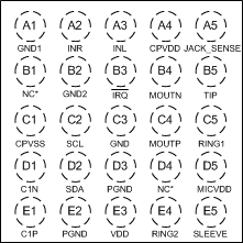
All NC pins should be left floating. Do not connect them to GND.

Pin Functions

PIN I/O / TYPE DESCRIPTION
NAME NO.
GND1 A1 P Analog / digital ground 1
INR A2 I Headphone right channel input
INL A3 I Headphone left channel input
CPVDD A4 I Headphone charge-pump positive supply (internally generated). Connect a 1-µF capacitor to ground.
JACK_SENSE A5 I/O Connect to headset jack terminal 5 (for mechanical switch). If mechanical switch is not available, then this terminal can be kept floating.
NC (Floating) B1 O Leave floating (no connection)
GND2 B2 I Ground 2 - Connect to ground 1 on board.
IRQ B3 O Active low interrupt output
MOUTN B4 O Microphone preamplifier negative output
TIP B5 O Left headphone / line output. Connect to headset jack TIP (terminal 1).
CPVSS C1 I Headphone charge-pump negative supply (internally generated). Connect a 1-µF capacitor to ground.
SCL C2 I I2C clock line
GND C3 I Connect to ground
MOUTP C4 O Microphone preamplifier positive output
RING1 C5 O Right headphone / line output. Connect to headset jack RING1 (terminal 2).
C1N D1 P Charge pump flying capacitor positive terminal
SDA D2 I/O I2C data line
PGND D3, E2 P Power ground
NC (Floating) D4 O Leave floating (no connection)
MICVDD D5 P Analog supply
C1P E1 P Charge pump flying capacitor negative terminal
VDD E3 P Analog / digital supply
RING2 E4 I/O Connect to headset jack RING2 (terminal 3)
SLEEVE E5 I/O Connect to headset jack SLEEVE (terminal 4)