SLAS997B March 2014 – January 2015 TPA6166A2
PRODUCTION DATA.
- 1 Features
- 2 Applications
- 3 Description
- 4 Revision History
- 5 Pin Configuration and Functions
- 6 Specifications
-
7 Detailed Description
- 7.1 Overview
- 7.2 Functional Block Diagram
- 7.3 Feature Description
- 7.4 Device Functional Modes
- 7.5
Register Maps
- 7.5.1 Register Functional Overview
- 7.5.2 Initialization
- 7.5.3 Typical Use Case Modes
- 7.5.4 Recommended Software Flow Chart
- 7.5.5 Register Map Summary
- 7.5.6
Detailed Register Descriptions
- 7.5.6.1 Register 0x00: Config and Device Status Register 1
- 7.5.6.2 Register 0x01: Config and Device Status Register 2
- 7.5.6.3 Register 0x02: Config and Device Status Register 2
- 7.5.6.4 Register 0x03: Reserved Register
- 7.5.6.5 Register 0x04: Interrupt Mask Register 1
- 7.5.6.6 Register 0x05: Interrupt Mask Register 2
- 7.5.6.7 Register 0x06: Reserved Register
- 7.5.6.8 Register 0x07: Headphone Volume Register 1
- 7.5.6.9 Register 0x08: Headphone Volume Control Register 2
- 7.5.6.10 Register 0x09: Microphone Bias Control Register
- 7.5.6.11 Register 0x0a: Reserved
- 7.5.6.12 Register 0x0b: Revision ID Register
- 7.5.6.13 Register 0x0c: Reserved Register
- 7.5.6.14 Registers 0x0d to 0x10: Reserved Registers
- 7.5.6.15 Register 0x11: Reserved
- 7.5.6.16 Register 0x12: Reserved
- 7.5.6.17 Register 0x13: Reserved
- 7.5.6.18 Register 0x14: Reserved Register
- 7.5.6.19 Register 0x15: Keyscan Debounce Register
- 7.5.6.20 Register 0x16: Keyscan Delay Register
- 7.5.6.21 Register 0x17: Passive Multi Button Keyscan Data Register
- 7.5.6.22 Register 0x18: Jack Detect Test Hardware Settings
- 7.5.6.23 Register 0x19:State Register
- 7.5.6.24 Register 0x1a: Jack Detect Test Hardware Settings
- 7.5.6.25 Registers 0x1b: Reserved
- 7.5.6.26 Register 0x1c: Clock Control
- 7.5.6.27 Register 0x1d: Enable Register 1
- 7.5.6.28 Register 0x1e: Enable Register 2
- 7.5.6.29 Register 0x1F: Reserved
- 7.5.6.30 Register 0x66: Clock Flex Register
- 7.5.6.31 Register 0x6F: Clock Set Register
- 8 Application and Implementation
- 9 Power Supply Recommendations
- 10Layout
- 11Device and Documentation Support
- 12Mechanical, Packaging, and Orderable Information
Package Options
Mechanical Data (Package|Pins)
- YFF|25
Thermal pad, mechanical data (Package|Pins)
Orderable Information
6 Specifications
6.1 Absolute Maximum Ratings
over operating temperature range, TA = 25°C (unless otherwise noted) (1)| MIN | MAX | UNIT | ||
|---|---|---|---|---|
| Supply voltage, VDD | –0.3 | 2 | V | |
| Microphone supply voltage, MICVDD | –0.3 | 3.9 | V | |
| Output continuous total power dissipation | See Thermal Information | |||
| Storage temperature, Tstg | –65 | 85 | °C | |
(1) Stresses beyond those listed under Absolute Maximum Ratings may cause permanent damage to the device. These are stress ratings only, which do not imply functional operation of the device at these or any other conditions beyond those indicated under Recommended Operating Conditions. Exposure to absolute-maximum-rated conditions for extended periods may affect device reliability.
6.2 ESD Ratings
| VALUE | UNIT | |||
|---|---|---|---|---|
| V(ESD) | Electrostatic discharge | Human body model (HBM), per ANSI/ESDA/JEDEC JS-001(1) | ±2000 | V |
| Charged-device model (CDM), per JEDEC specification JESD22-C101(2) | ±500 | |||
(1) JEDEC document JEP155 states that 500-V HBM allows safe manufacturing with a standard ESD control process.
(2) JEDEC document JEP157 states that 250-V CDM allows safe manufacturing with a standard ESD control process.
6.3 Recommended Operating Conditions
| MIN | MAX | UNIT | |||
|---|---|---|---|---|---|
| VDD | Supply voltage | 1.7 | 1.9 | V | |
| MICVDD | Microphone supply voltage | 2.4 | 3.6 | V | |
| TA | Operating temperature | –25 | 85 | °C | |
| CL,Max | Maximum load capacitance | Line Driver Application, RL = 10 kΩ, AV ≥ 0 dB, specified by design | 470 | pF | |
| Line Driver Application, RL = 10 kΩ, AV ≤ 0 dB, LO_EXT_STAB = 1, specified by design | 470 | ||||
| Headphone Application, RL = 32 Ω, specified by design | 200 | ||||
| TJ | Operating junction temperature | –25 | 150 | °C | |
6.4 Thermal Information
| THERMAL METRIC(1) | TPA6166A2 | UNIT | |
|---|---|---|---|
| YFF (WSCP) | |||
| 25 PINS | |||
| RθJA | Junction-to-ambient thermal resistance | 67 | °C/W |
| RθJC(top) | Junction-to-case (top) thermal resistance | 18 | |
| RθJB | Junction-to-board thermal resistance | 38 | |
| ψJT | Junction-to-top characterization parameter | 0.1 | |
| ψJB | Junction-to-board characterization parameter | 36 | |
(1) For more information about traditional and new thermal metrics, see the IC Package Thermal Metrics application report, SPRA953.
6.5 Electrical Characteristics
VDD =00 1.8 V, MICVDD = 3.0 V, AV = 0 dB, CIN = 0.47 µF, CFLY = 1.0 μF, CCPVDD = CCPVSS = 1.0 μF, RHP = 32 Ω, outputs in phase, TA = 25°C (unless otherwise noted).| PARAMETER | TEST CONDITIONS | MIN | TYP | MAX | UNIT | ||
|---|---|---|---|---|---|---|---|
| VIH | Input logic high | SDA, SCL | 1.4 | V | |||
| VIL | Input logic low | SDA, SCL | 0.4 | ||||
| VOL | Output logic low | IRQ | IOL = 3 mA pullup current | 0.2×VDD | |||
| |IIH| | Logic high input leakage current | SDA, SCL | 1 | µA | |||
| |IIL| | Logic low input leakage current | SDA, SCL | 1 | ||||
| |IOH| | Logic high output leakage current | IRQ | VIRQ = 3.3 V | 1 | |||
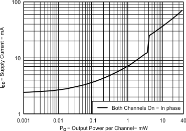
| Power consumption | Audio playback (both channels), no signal into 32 Ω | IVDD | 2.38 | mA | |||
| IMICVDD | 0.21 | mA | |||||
| PCONS(1) | 4.91 | mW | |||||
| Audio playback (both channels), 100-µW output into 32 Ω | IVDD | 3.74 | mA | ||||
| IMICVDD | 0.21 | mA | |||||
| PCONS(1) | 7.35 | mW | |||||
| 2-way call, no signal into 32 Ω | IVDD | 2.36 | mA | ||||
| IMICVDD | 0.96 | mA | |||||
| PCONS(1) | 6.35 | mW | |||||
| 2-way call, 100-µW output into 32 Ω | IVDD | 3.68 | mA | ||||
| IMICVDD | 0.96 | mA | |||||
| PCONS(1) | 8.74 | mW | |||||
| Accessory not inserted | IVDD | 10.84 | µA | ||||
| IMICVDD | 1.05 | µA | |||||
| PCONS(1) | 22.7 | µW | |||||
| Accessory not inserted, mechanical switch is open (JACK_SENSE=1) | IVDD | 150.9 | µA | ||||
| IMICVDD | 1.05 | µA | |||||
| PCONS(1) | 278.3 | µW | |||||
| Accessory inserted and in sleep mode | IVDD | 108.1 | µA | ||||
| IMICVDD | 1.06 | µA | |||||
| PCONS(1) | 197.8 | µW | |||||
(1) Total power consumption from VDD and MICVDD.
6.6 Electrical Characteristics, Audio Amplifiers
VDD = 1.8 V, MICVDD = 3.0 V, AV = 0 dB, CIN = 0.47 µF, CFLY = 1.0 μF, CCPVDD = CCPVSS = 1.0 μF, RL = 32 Ω, outputs in phase, TA = 25°C (unless otherwise noted).| PARAMETER | TEST CONDITIONS | MIN | TYP | MAX | UNIT | ||
|---|---|---|---|---|---|---|---|
| HEADPHONE AND LINE-OUT AMPLIFIERS | |||||||
| Programmable gain range | -42 | 6 | dB | ||||
| AV,Max | AV = 6 dB | 5.0 | 6.0 | 7.0 | dB | ||
| AV,Min | AV = -42 dB | -43 | -42 | -41 | dB | ||
| Gain step size | -42 dB ≤ AV ≤ 6 dB | 1 | dB | ||||
| ΔAV | Gain matching | Between left and right channels | –0.5 | 0.5 | dB | ||
| Mute attenuation | 103.7 | dB | |||||
| PO | Output power | THD+N = 1%, f = 1 kHz, RL = 32 Ω, single channel on | 29.1 | mW | |||
| THD+N = 1%, f = 1 kHz, RL = 32 Ω, C both channels on |
23.2 | ||||||
| THD+N = 1%, f = 1 kHz, RL = 16 Ω, single channel on | 43.0 | ||||||
| THD+N = 1%, f = 1 kHz, RL = 16 Ω, The processing of Request 596221 was completed at 10:19 on 28 Jan 2015. Click here to access the data Click here to access the HTML data both channels on | 30.2 | ||||||
| THD+N | Total harmonic distortion plus noise | RL = 16 Ω, PO = 10 mW, f = 1 kHz | 0.021% | ||||
| RL = 16 Ω, PO = 0.1 mW, f = 1 kHz | 0.057% | ||||||
| RL = 10 kΩ, VOUT = 1 VRMS, f = 1 kHz | 0.014% | ||||||
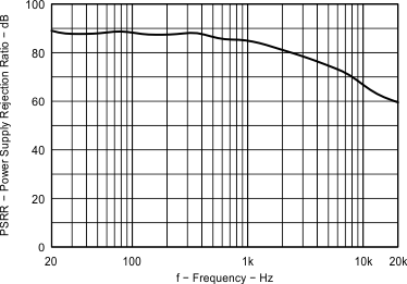
| PSRR | Power supply rejection ratio | f = dc, VDD = 1.7 V to 1.9 V, AV = 0 dB | 70 | 91 | dB | ||
| f = 217 Hz, 100 mVP-P ripple on VDD | 88 | ||||||
| f = 10 kHz, 100 mVP-P ripple on VDD | 71 | ||||||
| EN | Output noise(1) | AV = 0 dB | 8.0 | µVRMS | |||
| AV = -30 dB | 2.0 | ||||||
| AV = -42 dB | 2.0 | ||||||
| Crosstalk between left and right channels | RL = 16 Ω, f = 1 kHz, PO = 5 mW | –56 | dB | ||||
| RL = 32 Ω, f = 1 kHz, PO = 25 mW | –62 | ||||||
| RIN | Amplifier input resistance | 20 | kΩ | ||||
| VOOS | Output offset voltage | AV = 0 dB | –0.5 | 0.5 | mV | ||
| VOUT,Max | Max line output voltage | RL = 10 kΩ | 1 | VRMS | |||
| fC,LPF | Input low-pass filter 3-dB cutoff frequency(2) | AV = 0 dB | 45.1 | kHz | |||
| Low-pass filter passband gain(2) | f = 10 Hz to 15 kHz, dc-coupled inputs with VCM = 0 V | –0.4 | dB | ||||
| Low-pass filter stopband gain(2) | f = 145 kHz | –16 | dB | ||||
| fCP | Charge pump frequency | 1.3 | MHz | ||||
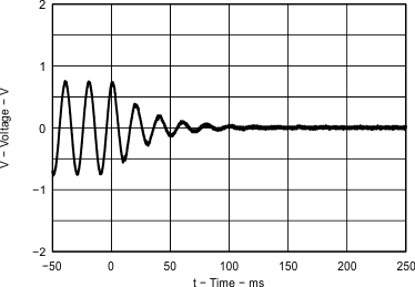
| Click and pop(1) | AV = 0 dB, Volume Slewing Enabled, RL = 32 Ω, peak voltage, 32 samples / second | Into shutdown | –83 | dBV | |||
| Out of shutdown | –69 | ||||||
| Power consumption(3) | PO = 0.5 mW, RL = 32 Ω | 6.2 | mW | ||||
| PO = 5 mW, RL = 32 Ω, THRH = 1 | 13.3 | ||||||
| PO = 30 mW, RL = 32 Ω, THRH = 0 | 56.9 | ||||||
| RL | Minimum headphone load | 32 | 7.8 | Ω | |||
(1) A-weighted
(2) Measured with respect to gain at 997 Hz
6.7 Electrical Characteristics, Mic Preamplifier and Bias
VDD = 1.8 V, MICVDD = 3.0 V, TA = 25°C (unless otherwise noted).| PARAMETER | TEST CONDITIONS | MIN | TYP | MAX | UNIT | ||
|---|---|---|---|---|---|---|---|
| MICROPHONE BIAS | |||||||
| VBIAS | Microphone bias voltage | Programmed for high value, MICVDD ≥ 2.8 V | 2.45 | 2.6 | 2.75 | V | |
| Programmed for low value | 1.88 | 2.0 | 2.12 | ||||
| IOUT | Max bias output current | Internal bias resistor bypassed (MICR = 011) | 1.2 | mA | |||
| RBIAS | Bias output resistance | MICR = 000 | 2.09 | 2.2 | 2.31 | kΩ | |
| MICR = 001 | 2.47 | 2.6 | 2.73 | ||||
| MICR = 010 | 2.85 | 3.0 | 3.15 | ||||
| MICR = 011 | 0.13 | ||||||
| EN | Bias output noise(1) | Between SLEEVE and RING2, BW = 100 Hz to 7 kHz, 2.2 kΩ load between SLEEVE and RING2, MICR = 000, VBIAS = 2.0 V | 2.0 | µVRMS | |||
| PSRR | Power supply rejection ratio | Measured between SLEEVE and RING2, 2.2 kΩ load between SLEEVE and RING2, MICR = 000, VBIAS = 2.6 V | f = dc, MICVDD = 2.8 V to 3.6 V | 92 | dB | ||
| f = 2 kHz, 100 mVP-P ripple, MICVDD = 3.0 V | 73 | ||||||
| f = 2 kHz, 100 mVP-P ripple, MICVDD = 2.8 V | 73 | ||||||
| MicZ | Microphone Capsule Impedance | Measured between Mic and GND before insertion | 1500 | 20000 | Ω | ||
| MICROPHONE PREAMPLIFIER | |||||||
| AV | Preamplifier gain | Programmed for high value, f = 997 Hz | 23 | 24 | 25 | dB | |
| Programmed for low value, f = 997 Hz | 11 | 12 | 13 | ||||
| EN | Input referred noise(1) | f = 100 Hz to 7 kHz, AV = 24 dB, Mic on SLEEVE, 2.2 kΩ load between SLEEVE and RING2, MICR = 000, VBIAS = 2.0 V | 3.4 | µVRMS | |||
| THD+N | Total harmonic distortion plus noise | VOUT = 1 VRMS | 0.095% | ||||
| PSRR | Power supply rejection ratio | Measured between MOUTP-MOUTN, 6.04 kΩ between SLEEVE and RING2, MICR = 010, VBIAS = 2.0 V, f = dc, MICVDD = 2.4 V to 3.6 V | 74 | dB | |||
| Measured between MOUTP-MOUTN, 2.2 kΩ between SLEEVE and RING2, MICR = 000, VBIAS = 2.6 V | f = dc, MICVDD = 2.8 V to 3.6 V | 109.5 | |||||
| f = 2 kHz, 100 mVP-P ripple on MICVDD | 78 | ||||||
| VCMO | Output Common Mode | MICVDD = 2.4 V – 3.6V | 0.4×MICVDD | V | |||
| fC,LO | Lower -3 dB frequency of HPF(2) | 20 | Hz | ||||
| fC,HI | Upper -3 dB frequency of amplifier(2) | 260 | kHz | ||||
(1) A-weighted
(2) Measured with respect to gain at 997 Hz
6.8 Timing Requirements
For I2C interface signals and voltage power-up sequence, over recommended operating conditions (unless otherwise noted). Timing is specified by design.| MIN | MAX | UNIT | |||
|---|---|---|---|---|---|
| fSCL | Frequency, SCL | No wait states | 400 | kHz | |
| tw(H) | Pulse duration, SCL high | 0.6 | μs | ||
| tw(L) | Pulse duration, SCL low | 1.3 | μs | ||
| tsu1 | Setup time, SDA to SCL | 100 | ns | ||
| th1 | Hold time, SCL to SDA | 10 | ns | ||
| t(buf) | Bus free time between stop and start condition | 1.3 | μs | ||
| tsu2 | Setup time, SCL to start condition | 0.6 | μs | ||
| th2 | Hold time, start condition to SCL | 0.6 | μs | ||
| tsu3 | Setup time, SCL to stop condition | 0.6 | μs | ||
| tSP | Pulse width of surpressed spike | 0 | 50 | ns | |
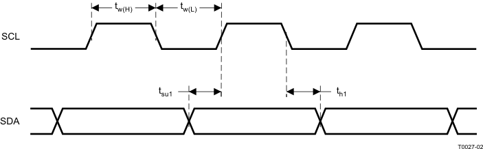 Figure 1. SCL and SDA Timing
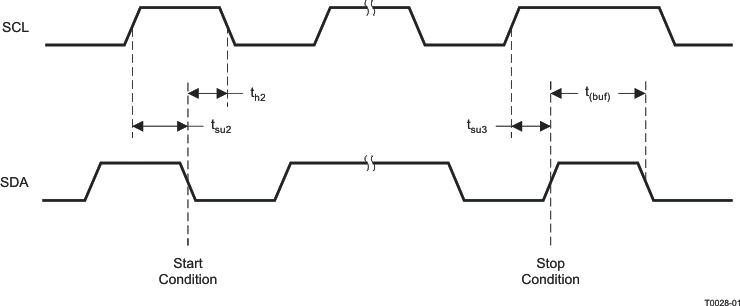 Figure 2. Start and Stop Conditions Timing
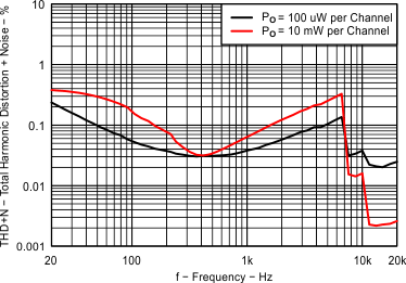
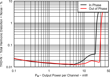
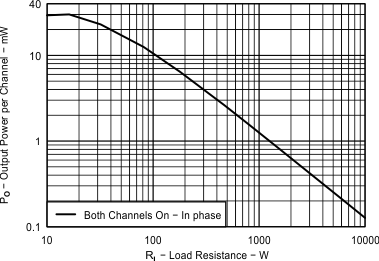
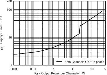
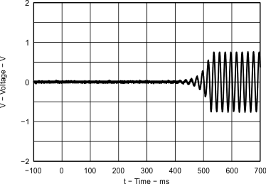
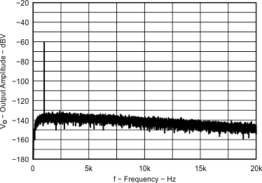
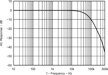
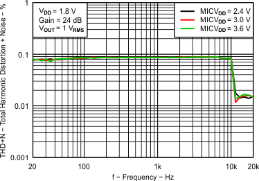
6.9 Typical Characteristics
VDD = 1.8 V, MICVDD = 3.0 V, AV = 0 dB, CIN = 0.47 µF, CFLY = 1.0 μF, CCPVDD = CCPVSS = 1.0 μF, RHP = 32 Ω, outputs in phase, TA = 25°C (unless otherwise noted).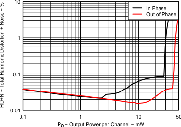
| VDD = 1.8 V | RL = 16 Ω | Gain = 0 dB |
| f - 1 kHz | ||
| VDD = 1.8 V | RL = 16 Ω | Gain = 0 dB |
| VDD = 1.8 V | RL = 16 Ω | Gain = 0 dB |
| VDD = 1.8 V | RL = 32 Ω | Gain = 0 dB |
| f = 1kHz | THRH = 0 | |
| VIN = 0.5 VRMS | RL = 16 Ω | |
| Volume slewing enabled | ||
| Device enabled at 0 ms | ||
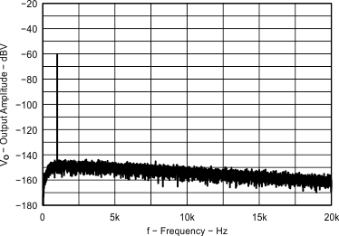
| VDD = 1.8 V | RL = 16 Ω | Gain = –30 dB |
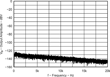
| A weighted | ||
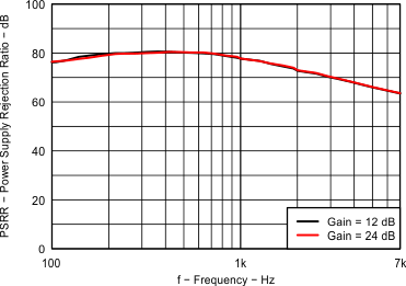
| VDD = 1.8 V | VOUT = 1 VRMS | Gain = 12 dB |
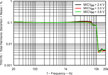
| MIC VDD = 3.0 V | Gain = 12 dB | |
| VDD = 1.8 V | MIC VDD = 3.0 V | |
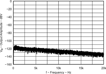
| MIC VDD = 3.0 V | Gain = 24 dB | No signal input | ||
| VDD = 1.8 V | RL = 32 Ω | Gain = 0 dB |
| f - 1 kHz | ||
| VDD = 1.8 V | f = 1 kHz | Gain = 0 dB |
| THD+N = 1% | ||
| VDD = 1.8 V | RL = 16 Ω | Gain = 0 dB |
| f = 1kHz | THRH = 0 | |
| VIN = 0.5 VRMS | RL = 16 Ω | |
| Volume slewing enabled | ||
| Device enabled at 0 ms | ||
| VDD = 1.8 V | RL = 16 Ω | Gain = 0 dB |
| A weighted | ||
| VDD = 1.8 V | RL = 16 Ω | Gain = 0 dB |
| VDD = 1.8 V | VOUT = 1 VRMS | Gain = 24 dB |
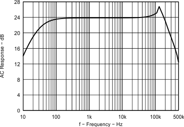
| MIC VDD = 3.0 V | Gain = 24 dB | |
| MIC VDD = 3.0 V | Gain = 12 dB | No signal input |