SLUSCE3C October 2015 – August 2020 TPS2549-Q1
PRODUCTION DATA
- 1 Features
- 2 Applications
- 3 Description
- 4 Revision History
- 5 Pin Configuration and Functions
- 6 Specifications
- 7 Parameter Measurement Information
-
8 Detailed Description
- 8.1 Overview
- 8.2 Functional Block Diagram
- 8.3 Feature Description
- 8.4 Device Functional Modes
- 9 Application and Implementation
- 10Power Supply Recommendations
- 11Layout
- 12Device and Documentation Support
- 13Mechanical, Packaging, and Orderable Information
Package Options
Mechanical Data (Package|Pins)
- RTE|16
Thermal pad, mechanical data (Package|Pins)
- RTE|16
Orderable Information
8.3.10 Current Limit Setting
The TPS2549-Q1 has two independent current-limit settings that are each programmed externally with a resistor. The ILIM_HI setting is programmed with R(ILIM_HI) connected between ILIM_HI and GND. The ILIM_LO setting is programmed with R(ILIM_LO) connected between ILIM_LO and GND. Consult the device truth table (Table 8-2) to see when each current limit is used. Both settings have the same relation between the current limit and the programming resistor.
R(ILIM_LO) is optional and the ILIM_LO pin may be left unconnected if the following conditions are met:
- The TPS2549-Q1 device is configured as DCP(001) or CDP(111).
- Load detection is not used.
The following equation calculates the value of resistor for programming the typical current limit:
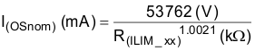
R(ILIM_xx) corresponds to either R(ILIM_HI) or R(ILIM_LO), as appropriate.
Many applications require that the current limit meet specific tolerance limits. When designing to these tolerance limits, both the tolerance of the TPS2549-Q1 current limit and the tolerance of the external programming resistor must be taken into account. The following equations approximate the TPS2549-Q1 minimum and maximum current limits to within a few milliamperes and are appropriate for design purposes. The equations do not constitute part of TI’s published device specifications for purposes of TI’s product warranty. These equations assume an ideal—no variation—external programming resistor. To take resistor tolerance into account, first determine the minimum and maximum resistor values based on its tolerance specifications and use these values in the equations. Because of the inverse relation between the current limit and the programming resistor, use the maximum resistor value in the I(OS_min) equation and the minimum resistor value in the I(OS_max) equation.
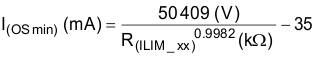
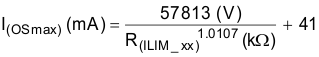
 Figure 8-6 Current Limit Setting vs Programming Resistor I
 Figure 8-7 Current Limit Setting vs Programming Resistor II
The routing of the traces to the R(ILIM_xx) resistors should have a sufficiently low resistance so as to not affect the current-limit accuracy. The ground connection for the R(ILIM_xx) resistors is also very important. The resistors must reference back to the TPS2549-Q1 GND pin. Follow normal board layout practices to ensure that current flow from other parts of the board does not impact the ground potential between the resistors and the TPS2549-Q1 GND pin.