SLUSCE3C October 2015 – August 2020 TPS2549-Q1
PRODUCTION DATA
- 1 Features
- 2 Applications
- 3 Description
- 4 Revision History
- 5 Pin Configuration and Functions
- 6 Specifications
- 7 Parameter Measurement Information
-
8 Detailed Description
- 8.1 Overview
- 8.2 Functional Block Diagram
- 8.3 Feature Description
- 8.4 Device Functional Modes
- 9 Application and Implementation
- 10Power Supply Recommendations
- 11Layout
- 12Device and Documentation Support
- 13Mechanical, Packaging, and Orderable Information
Package Options
Mechanical Data (Package|Pins)
- RTE|16
Thermal pad, mechanical data (Package|Pins)
- RTE|16
Orderable Information
9.2.2.3 Power Dissipation and Junction Temperature
The low on-resistance of the N-channel MOSFET allows small surface-mount packages to pass large currents. It is good design practice to estimate power dissipation and junction temperature. The following analysis gives an approximation for calculating junction temperature based on the power dissipation in the package. However, it is important to note that thermal analysis is strongly dependent on additional system-level factors. Such factors include air flow, board layout, copper thickness and surface area, and proximity to other devices dissipating power. Good thermal design practice must include all system-level factors in addition to individual component analysis. Begin by determining the rDS(on) of the N-channel MOSFET relative to the input voltage and operating temperature. As an initial estimate, use the highest operating ambient temperature of interest and read rDS(on) from the typical characteristics graph. Using this value, the power dissipation can be calculated by:
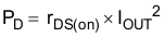
where:
PD = Total power dissipation (W)
rDS(on) = Power-switch on-resistance (Ω)
IOUT = Maximum current-limit threshold (A)
This step calculates the total power dissipation of the N-channel MOSFET.
Finally, calculate the junction temperature:
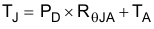
where:
TA = Ambient temperature (°C)
RθJA = Thermal resistance (°C/W)
PD = Total power dissipation (W)
Compare the calculated junction temperature with the initial estimate. If they are not within a few degrees, repeat the calculation using the refined rDS(on) from the previous calculation as the new estimate. Two or three iterations are generally sufficient to achieve the desired result. The final junction temperature is highly dependent on thermal resistance RθJA, and thermal resistance is highly dependent on the individual package and board layout.