SLUSCE3C October   2015  – August 2020 TPS2549-Q1

PRODUCTION DATA  

  1. Features
  2. Applications
  3. Description
  4. Revision History
  5. Pin Configuration and Functions
  6. Specifications
    1. 6.1 Absolute Maximum Ratings
    2. 6.2 ESD Ratings
    3. 6.3 Recommended Operating Conditions
    4. 6.4 Thermal Information
    5. 6.5 Electrical Characteristics
    6. 6.6 Switching Characteristics
    7. 6.7 Typical Characteristics
  7. Parameter Measurement Information
  8. Detailed Description
    1. 8.1 Overview
    2. 8.2 Functional Block Diagram
    3. 8.3 Feature Description
      1. 8.3.1  FAULT Response
      2. 8.3.2  Cable Compensation
        1. 8.3.2.1 Design Procedure
      3. 8.3.3  D+ and D– Protection
      4. 8.3.4  Output and D+ or D– Discharge
      5. 8.3.5  Port Power Management (PPM)
        1. 8.3.5.1 Benefits of PPM
        2. 8.3.5.2 PPM Details
        3. 8.3.5.3 Implementing PPM in a System With Two Charging Ports (CDP and SDP1)
        4. 8.3.5.4 Implementing PPM in a System With Two Charging Ports (DCP and DCP1)
      6. 8.3.6  CDP and SDP Auto Switch
      7. 8.3.7  Overcurrent Protection
      8. 8.3.8  Undervoltage Lockout
      9. 8.3.9  Thermal Sensing
      10. 8.3.10 Current Limit Setting
    4. 8.4 Device Functional Modes
      1. 8.4.1 Device Truth Table (TT)
      2. 8.4.2 USB Specification Overview
      3. 8.4.3 Standard Downstream Port (SDP) Mode — USB 2.0 and USB 3.0
      4. 8.4.4 Charging Downstream Port (CDP) Mode
      5. 8.4.5 Dedicated Charging Port (DCP) Mode
        1. 8.4.5.1 DCP BC1.2 and YD/T 1591-2009
        2. 8.4.5.2 DCP Divider-Charging Scheme
        3. 8.4.5.3 DCP 1.2-V Charging Scheme
      6. 8.4.6 DCP Auto Mode
      7. 8.4.7 Client Mode
      8. 8.4.8 High-Bandwidth Data-Line Switches
  9. Application and Implementation
    1. 9.1 Application Information
    2. 9.2 Typical Application
      1. 9.2.1 Design Requirements
      2. 9.2.2 Detailed Design Procedure
        1. 9.2.2.1 Input and Output Capacitance
        2. 9.2.2.2 Cable Compensation Calculation
        3. 9.2.2.3 Power Dissipation and Junction Temperature
    3. 9.3 Application Curves
  10. 10Power Supply Recommendations
  11. 11Layout
    1. 11.1 Layout Guidelines
    2. 11.2 Layout Example
  12. 12Device and Documentation Support
    1. 12.1 Documentation Support
      1. 12.1.1 Related Documentation
    2. 12.2 Receiving Notification of Documentation Updates
    3. 12.3 Support Resources
    4. 12.4 Trademarks
    5. 12.5 Electrostatic Discharge Caution
    6. 12.6 Glossary
  13. 13Mechanical, Packaging, and Orderable Information

Package Options

Mechanical Data (Package|Pins)
Thermal pad, mechanical data (Package|Pins)
Orderable Information

Cable Compensation

When a load draws current through a long or thin wire, there is an IR drop that reduces the voltage delivered to the load. In the vehicle from the voltage regulator 5-V output to the VPD_IN (input voltage of portable device), the total resistance of power switch rDS(on) and cable resistance causes an IR drop at the PD input.. So the charging current of most portable devices is less than their expected maximum charging current.
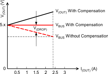
GUID-950A22A3-8643-476E-9593-E72929388AB7-low.gifFigure 8-1 Voltage Drop

TPS2549-Q1 device detects the load current and generates a proportional sink current that can be used to adjust output voltage of the upstream regulator to compensate the IR drop in the charging path. The gain G(CS) of the sink current proportional to load current is 75 µA/A.
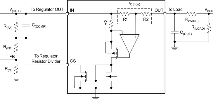
GUID-6DBF4E55-C9DE-4541-85F0-48BF4644A0F3-low.gifFigure 8-2 Cable Compensation Equivalent Circuit