SLVSDG2G July 2016 – December 2019 TPS2660
PRODUCTION DATA.
- 1 Features
- 2 Applications
- 3 Description
- 4 Revision History
- 5 Device Comparison Table
- 6 Pin Configuration and Functions
- 7 Specifications
- 8 Parameter Measurement Information
-
9 Detailed Description
- 9.1 Overview
- 9.2 Functional Block Diagram
- 9.3
Feature Description
- 9.3.1 Undervoltage Lockout (UVLO)
- 9.3.2 Overvoltage Protection (OVP)
- 9.3.3 Reverse Input Supply Protection
- 9.3.4 Hot Plug-In and In-Rush Current Control
- 9.3.5 Overload and Short Circuit Protection
- 9.4 Device Functional Modes
-
10Application and Implementation
- 10.1 Application Information
- 10.2
Typical Application
- 10.2.1 Design Requirements
- 10.2.2 Detailed Design Procedure
- 10.2.3 Application Curves
- 10.3 System Examples
- 10.4 Do's and Don'ts
- 11Power Supply Recommendations
- 12Layout
- 13Device and Documentation Support
- 14Mechanical, Packaging, and Orderable Information
- 14Mechanical, Packaging, and Orderable Information
Package Options
Refer to the PDF data sheet for device specific package drawings
Mechanical Data (Package|Pins)
- RHF|24
- PWP|16
Thermal pad, mechanical data (Package|Pins)
Orderable Information
3 Description
The TPS2660x devices are compact, feature rich high voltage eFuses with a full suite of protection features. The wide supply input range of 4.2 to 60 V allows control of many popular DC bus voltages. The device can withstand and protect the loads from positive and negative supply voltages up to ±60 V. Integrated back to back FETs provide reverse current blocking feature making the device suitable for systems with output voltage holdup requirements during power fail and brownout conditions. Load, source and device protection are provided with many adjustable features including overcurrent, output slew rate and overvoltage, undervoltage thresholds. The internal robust protection control blocks along with the high voltage rating of the TPS2660x helps to simplify the system designs for Surge protection.
A shutdown pin provides external control for enabling and disabling the internal FETs as well as placing the device in a low current shutdown mode. For system status monitoring and downstream load control, the device provides fault and precise current monitor output. The MODE pin allows flexibility to configure the device between the three current-limiting fault responses (circuit breaker, latch off, and Auto-retry modes).
The devices are available in a 5-mm × 4.4-mm 16-pin HTSSOP as well as 5-mm x 4-mm 24-pin VQFN package and are specified over a –40°C to +125°C temperature range.
Device Information(1)
| PART NUMBER | PACKAGE | BODY SIZE (NOM) |
|---|---|---|
| TPS26600
TPS26602 |
HTSSOP (16) | 5.00 mm × 4.40 mm |
| TPS26600
TPS26601 TPS26602 |
VQFN (24) | 5.00 mm × 4.00 mm |
- For all available packages, see the orderable addendum at the end of the data sheet.
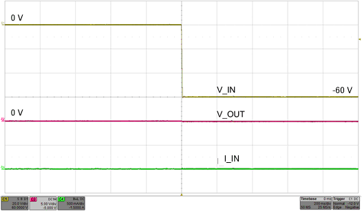
Reverse Input Polarity Protection at –60-V Supply
