SLVSDG2G July   2016  – December  2019 TPS2660

PRODUCTION DATA.  

  1. Features
  2. Applications
    1.     Simplified Schematic
  3. Description
    1.     Reverse Input Polarity Protection at –60-V Supply
  4. Revision History
  5. Device Comparison Table
  6. Pin Configuration and Functions
    1.     Pin Functions
  7. Specifications
    1. 7.1 Absolute Maximum Ratings
    2. 7.2 ESD Ratings
    3. 7.3 Recommended Operating Conditions
    4. 7.4 Thermal Information
    5. 7.5 Electrical Characteristics
    6. 7.6 Timing Requirements
    7. 7.7 Typical Characteristics
  8. Parameter Measurement Information
  9. Detailed Description
    1. 9.1 Overview
    2. 9.2 Functional Block Diagram
    3. 9.3 Feature Description
      1. 9.3.1 Undervoltage Lockout (UVLO)
      2. 9.3.2 Overvoltage Protection (OVP)
      3. 9.3.3 Reverse Input Supply Protection
      4. 9.3.4 Hot Plug-In and In-Rush Current Control
      5. 9.3.5 Overload and Short Circuit Protection
        1. 9.3.5.1 Overload Protection
          1. 9.3.5.1.1 Active Current Limiting
          2. 9.3.5.1.2 Electronic Circuit Breaker with Overload Timeout, MODE = OPEN
        2. 9.3.5.2 Short Circuit Protection
          1. 9.3.5.2.1 Start-Up With Short-Circuit On Output
        3. 9.3.5.3 FAULT Response
          1. 9.3.5.3.1 Look Ahead Overload Current Fault Indicator
        4. 9.3.5.4 Current Monitoring
        5. 9.3.5.5 IN, OUT, RTN, and GND Pins
        6. 9.3.5.6 Thermal Shutdown
        7. 9.3.5.7 Low Current Shutdown Control (SHDN)
    4. 9.4 Device Functional Modes
  10. 10Application and Implementation
    1. 10.1 Application Information
    2. 10.2 Typical Application
      1. 10.2.1 Design Requirements
      2. 10.2.2 Detailed Design Procedure
        1. 10.2.2.1 Step by Step Design Procedure
        2. 10.2.2.2 Programming the Current-Limit Threshold—R(ILIM) Selection
        3. 10.2.2.3 Undervoltage Lockout and Overvoltage Set Point
        4. 10.2.2.4 Programming Current Monitoring Resistor—RIMON
        5. 10.2.2.5 Setting Output Voltage Ramp Time—(tdVdT)
          1. 10.2.2.5.1 Case 1: Start-Up Without Load—Only Output Capacitance C(OUT) Draws Current During Start-Up
          2. 10.2.2.5.2 Case 2: Start-Up With Load—Output Capacitance C(OUT) and Load Draws Current During Start-Up
          3. 10.2.2.5.3 Support Component Selections—RFLTb and C(IN)
      3. 10.2.3 Application Curves
    3. 10.3 System Examples
      1. 10.3.1 Acive ORing Operation
      2. 10.3.2 Field Supply Protection in PLC, DCS I/O Modules
      3. 10.3.3 Simple 24-V Power Supply Path Protection
    4. 10.4 Do's and Don'ts
  11. 11Power Supply Recommendations
    1. 11.1 Transient Protection
  12. 12Layout
    1. 12.1 Layout Guidelines
    2. 12.2 Layout Example
  13. 13Device and Documentation Support
    1. 13.1 Device Support
    2. 13.2 Documentation Support
      1. 13.2.1 Related Documentation
    3. 13.3 Receiving Notification of Documentation Updates
    4. 13.4 Community Resources
    5. 13.5 Trademarks
    6. 13.6 Electrostatic Discharge Caution
    7. 13.7 Glossary
  14. 14Mechanical, Packaging, and Orderable Information
  15. 14Mechanical, Packaging, and Orderable Information

Package Options

Refer to the PDF data sheet for device specific package drawings

Mechanical Data (Package|Pins)
  • RHF|24
  • PWP|16
Thermal pad, mechanical data (Package|Pins)
Orderable Information

Typical Characteristics

–40°C ≤ TA = TJ ≤ +125°C, V(IN) = 24 V, V(SHDN)= 2 V, R(ILIM) = 120 kΩ, IMON = FLT = OPEN, C(OUT) = 1 μF, C(dVdT) = OPEN. (Unless stated otherwise)
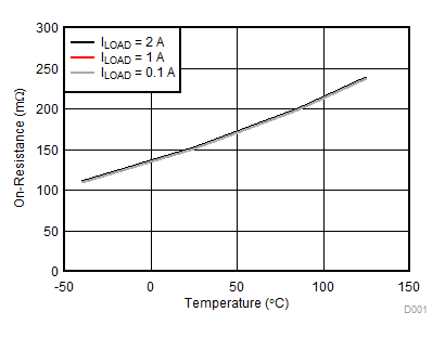
TPS2660 D001_SLVSDG2.gif
Figure 1. On-Resistance vs Temperature Across Load Current
TPS2660 D003_SLVSDG2.gif
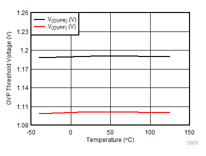
Figure 3. OVP Threshold Voltage vs Temperature
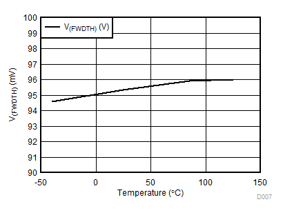
TPS2660 D007_SLVSDG2.gif
Figure 5. V(FWDTH) vs Temperature
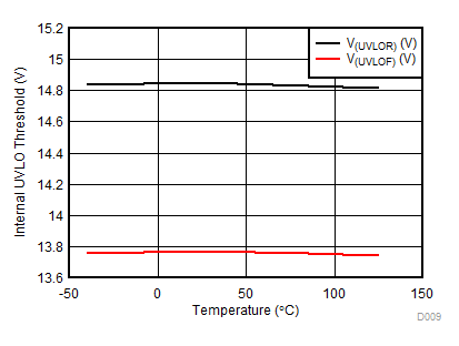
TPS2660 D009_SLVSDG2.gif
Figure 7. Internal UVLO Threshold vs Temperature
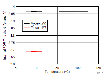
TPS2660 D012_SLVSDG2.gif
Figure 9. Internal POR Threshold Voltage vs Temperature
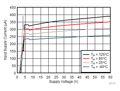
TPS2660 D014_SLVSDG2.gif
Figure 11. Input Supply Current vs Supply Voltage During Normal Operation
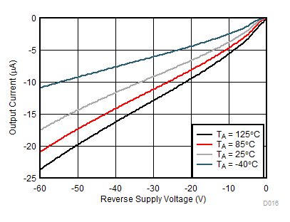
TPS2660 D016_SLVSDG2.gif
V(OUT) = 0 V
Figure 13. Output Current vs Reverse Supply Voltage, – V(IN)
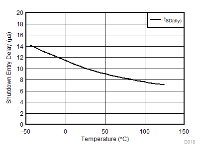
TPS2660 D018_SLVSDG2.gif
Figure 15. Shutdown Entry Delay vs Temperature
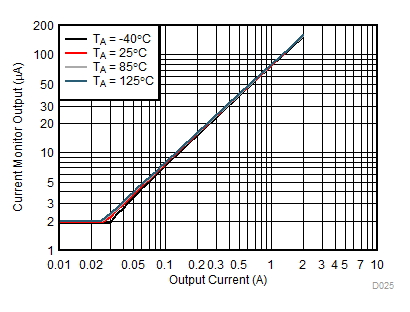
TPS2660 D025_SLVSDG2.gif
Figure 17. Current Monitor Output vs Output Current
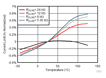
TPS2660 D021_SLVSDG2.gif
Figure 19. Current Limit (% Normalized) vs Temperature
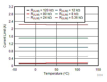
TPS2660 D004_SLVSDG2.gif
Figure 21. Over Load Current Limit vs Temperature
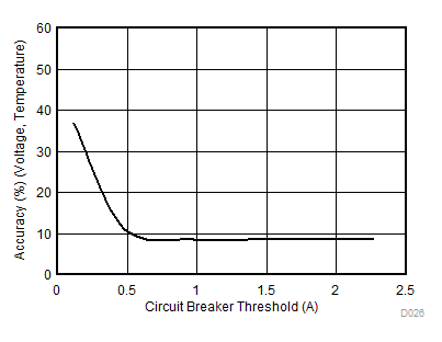
TPS2660 D026_SLVSDG2.gif
Figure 23. Circuit Breaker Threshold Accuracy vs Circuit Breaker Threshold I(CB)
TPS2660 D022_SLVSDG2.gif
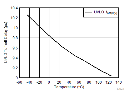
Figure 25. UVLO Turnoff Delay vs Temperature
TPS2660 scope_shot_09_slvsdg2.png
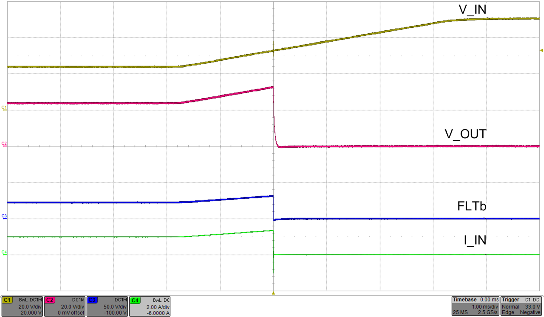
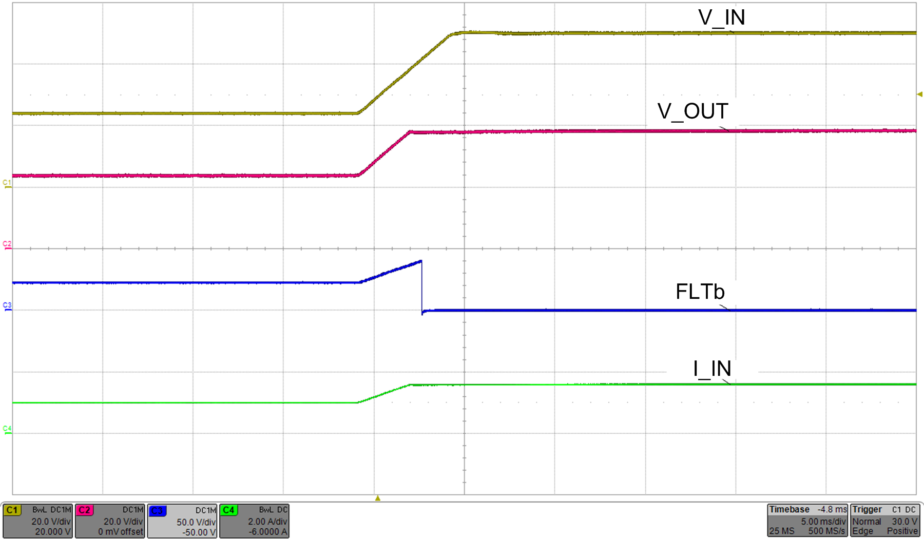
RILIM = 5.36 kΩ OVP Connected to RTN RFLTb = 100 kΩ RLOAD = 24 Ω
Figure 27. OVP Overvoltage Cut-Off Response
TPS2660 scope_shot_11_slvsdg2.png
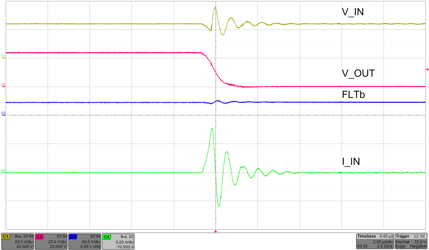
RILIM = 5.36 kΩ RFLTb = 100 kΩ
Figure 29. Hot-Short: Fast Trip Response and Current Regulation
TPS2660 scope_shot_14_slvsdg2.png
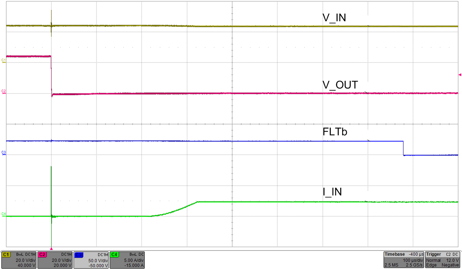
RILIM = 5.36 kΩ RFLTb = 100 kΩ RLOAD = 24 Ω
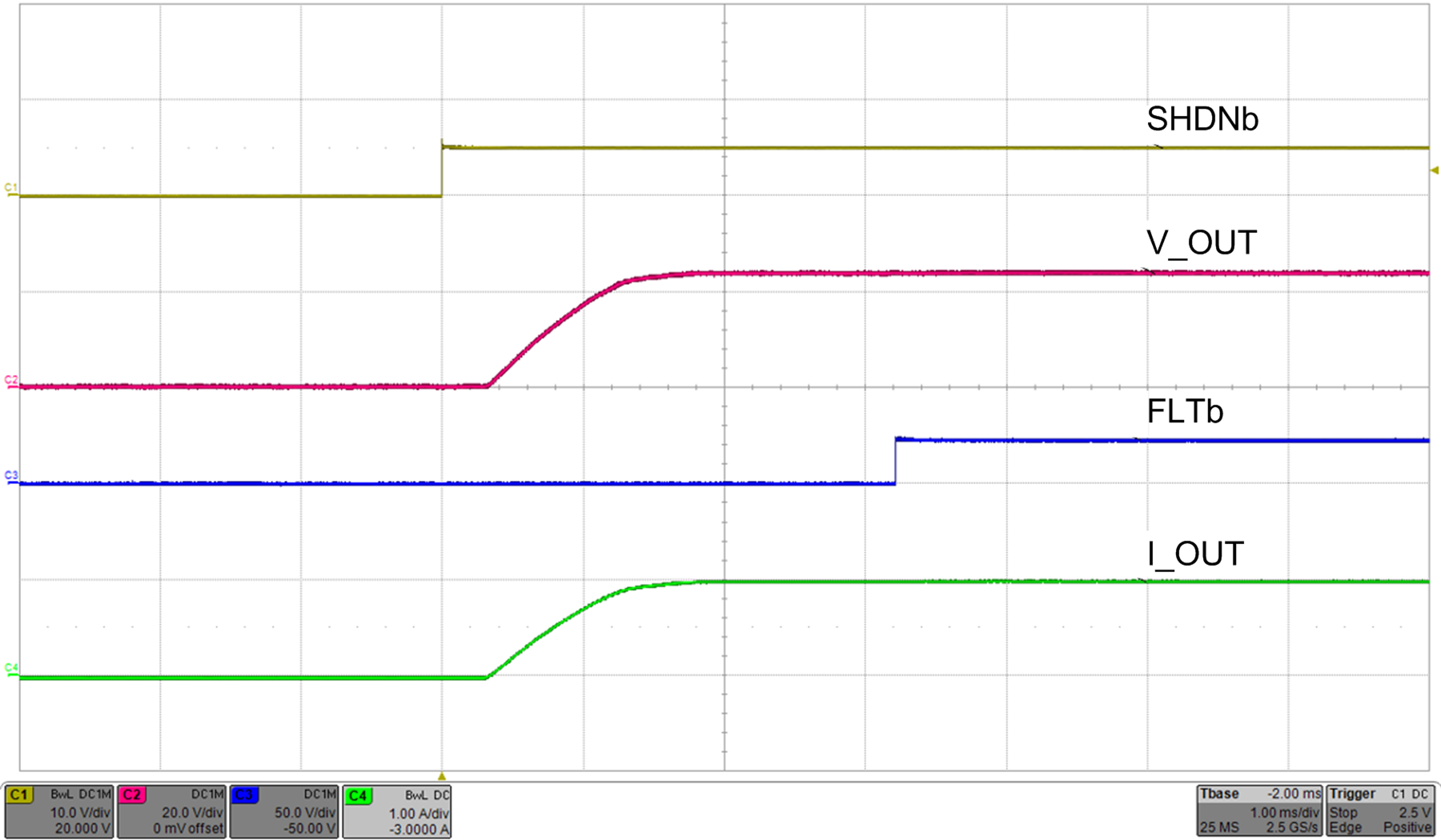
Figure 31. Turnon Control With SHDN
TPS2660 D002_SLVSDG2.gif
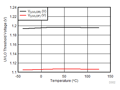
Figure 2. UVLO Threshold Voltage vs Temperature
TPS2660 D006_SLVSDG2.gif
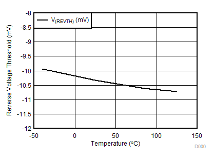
Figure 4. Reverse Voltage Threshold vs Temperature
TPS2660 D008_SLVSDG2.gif
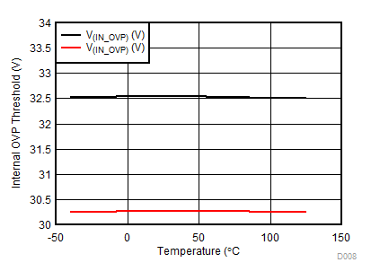
Figure 6. Internal OVP Threshold vs Temperature
TPS2660 D010_SLVSDG2.gif
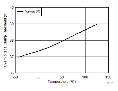
Figure 8. Overvoltage Clamp Threshold vs Temperature
TPS2660 D013_SLVSDG2.gif
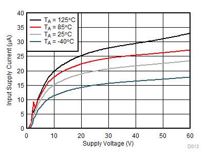
Figure 10. Input Supply Current vs Supply Voltage in Shutdown
TPS2660 D015_SLVSDG2.gif
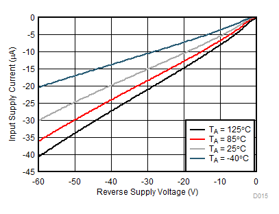
V(OUT) = 0 V
Figure 12. Input Supply Current vs Reverse Supply Voltage, – V(IN)
TPS2660 D017_SLVSDG2.gif
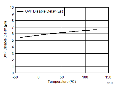
Figure 14. OVP Disable Delay vs Temperature
TPS2660 D019_SLVSDG2.gif
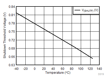
Figure 16. Shutdown Threshold Voltage Shutdown vs Temperature
TPS2660 D020_SLVSDG2.gif
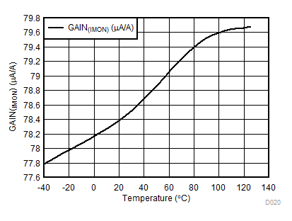
Figure 18. GAIN(IMON) vs Temperature
TPS2660 D024_SLVSDG2.gif
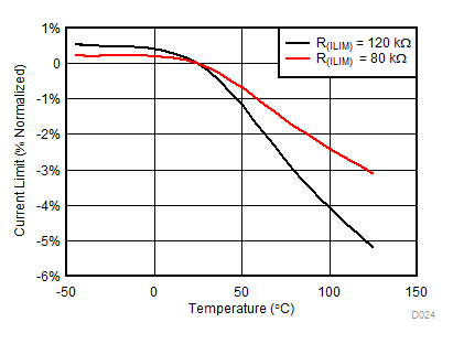
Figure 20. Current Limit (% Normalized) vs Temperature
TPS2660 D005_SLVSDG2.gif
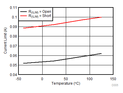
Figure 22. Current Limit for R(ILIM) = Open and Short vs Temperature
TPS2660 D027_SLVSDG2.gif
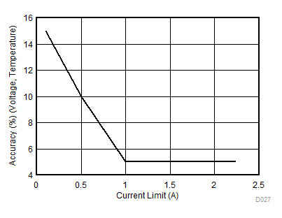
Figure 24. Current Limit Accuracy vs Current Limit, I(OL)
TPS2660 D023_SLVSDG2.gif
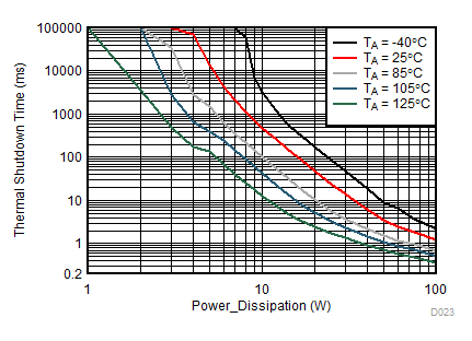
Taken on 2-Layer board, 2 oz.(0.08-mm thick) with HTSSOP device with RTN plane area: 1 cm2 (Top) and 4.6 cm2 (Bottom)
Figure 26. Thermal Shutdown Time vs Power Dissipation
TPS2660 scope_shot_06_slvsdg2.png
RILIM = 5.36 kΩ RFLTb = 100 kΩ RLOAD = 24 Ω
Figure 28. OV Clamp Response (TPS26602 Only)
TPS2660 scope_shot_12_slvsdg2.png
RILIM = 5.36 kΩ
Figure 30. Hot-Short: Fast Trip Response (Zoomed)
TPS2660 scope_shot_13_slvsdg2.png
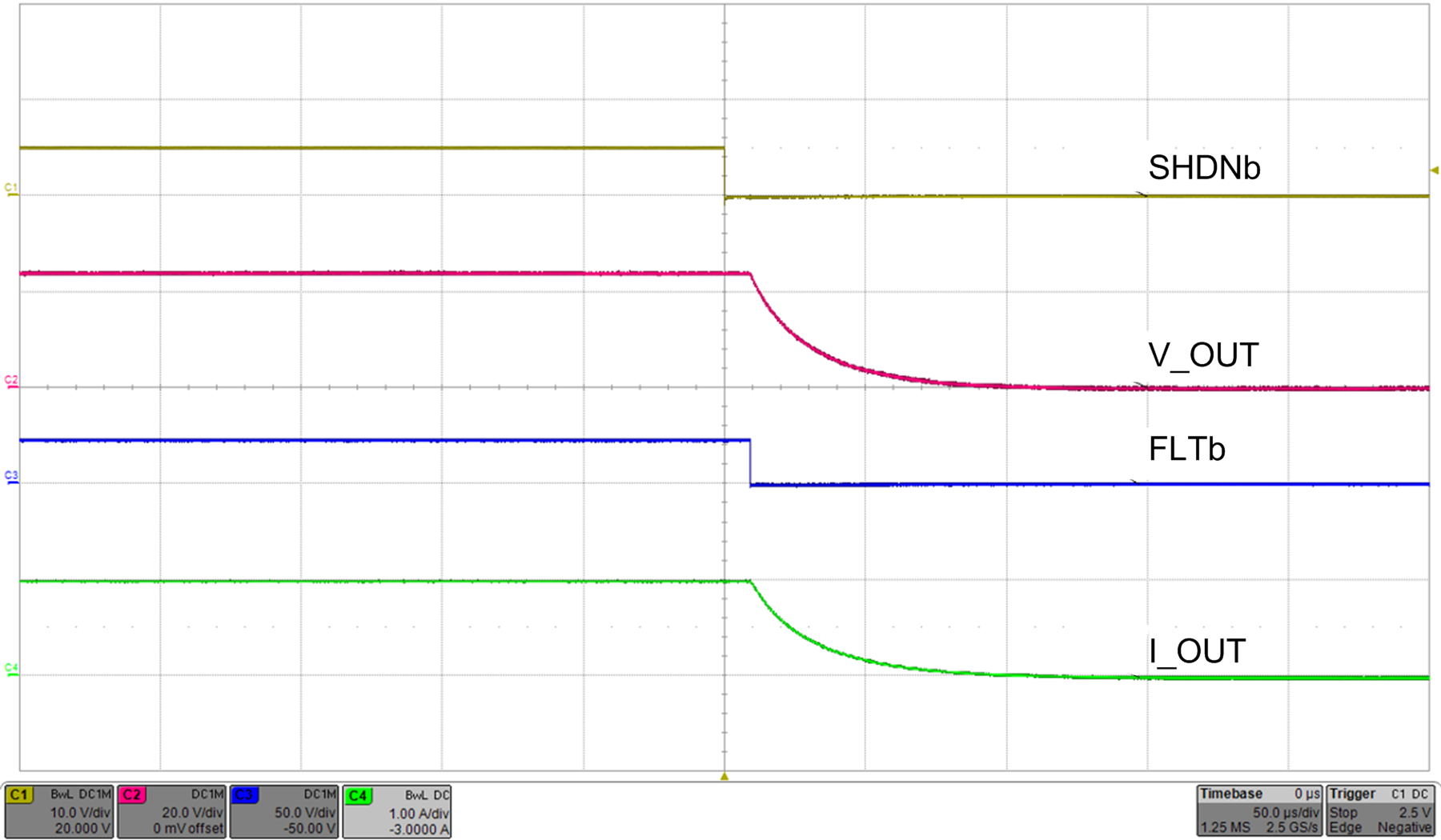
RILIM = 5.36 kΩ RFLTb = 100 kΩ RLOAD = 24 Ω
Figure 32. Turnoff Control With SHDN