SLVSE94F September 2018 – June 2021 TPS2663
PRODUCTION DATA
- 1 Features
- 2 Applications
- 3 Description
- 4 Revision History
- 5 Device Comparison Table
- 6 Pin Configuration and Functions
- 7 Specifications
- 8 Parameter Measurement Information
-
9 Detailed Description
- 9.1 Overview
- 9.2 Functional Block Diagram
- 9.3
Feature Description
- 9.3.1 Hot Plug-In and In-Rush Current Control
- 9.3.2 PGOOD and PGTH
- 9.3.3 Undervoltage Lockout (UVLO)
- 9.3.4 Overvoltage Protection (OVP)
- 9.3.5 Input Reverse Polarity Protection (B_GATE, DRV)
- 9.3.6 Reverse Current Protection
- 9.3.7 Overload and Short Circuit Protection
- 9.3.8 Output Power Limiting, PLIM (TPS26632, TPS26633, TPS26635 and TPS26636 Only)
- 9.3.9 Current Monitoring Output (IMON)
- 9.3.10 FAULT Response ( FLT)
- 9.3.11 IN_SYS, IN, OUT and GND Pins
- 9.3.12 Thermal Shutdown
- 9.3.13 Low Current Shutdown Control (SHDN)
- 9.4 Device Functional Modes
-
10Application and Implementation
- 10.1 Application Information
- 10.2
Typical Application: Power Path Protection in a PLC System
- 10.2.1 Design Requirements
- 10.2.2 Detailed Design Procedure
- 10.2.3 Application Curves
- 10.3 System Examples
- 10.4 Do's and Don'ts
- 11Power Supply Recommendations
- 12Layout
- 13Device and Documentation Support
- 14Mechanical, Packaging, and Orderable Information
Package Options
Refer to the PDF data sheet for device specific package drawings
Mechanical Data (Package|Pins)
- RGE|24
- PWP|20
Thermal pad, mechanical data (Package|Pins)
Orderable Information
9.3.6 Reverse Current Protection
The device monitors V(IN_SYS) and V(OUT) to provide true reverse current blocking when a reverse condition or input power failure condition is detected. The reverse comparator turns OFF the external blocking FET Q1 quickly as soon as V(IN_SYS) – V(OUT) falls below –1 V. The total time taken to turn OFF the FET Q1 in this condition is tRCB(fast_dly) + t(Driver). The delay due to the driver stage t(Driver) can be calculated using Equation 4.
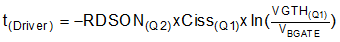
where
- RDSON(Q2) is the on resistance of the fast pull down switch Q2
- Ciss(Q1) is the input capacitance of the blocking FET Q1
- VGTH(Q1) is the GATE threshold voltage of the blocking FET Q1
- VBGATE = 10.2 V (typical)
In a typical system design, t(Driver) is generally 10% to 20% of tRCB(fast_dly) of 120 nsec (typical).
Figure 9-8 and Figure 9-9 illustrates the behavior of the system during input hot short circuit condition. The blocking FET Q1 is turned ON within 1.6 ms (typical) once the differential forward voltage V(IN_SYS) – V(OUT) exceeds 67 mV (typical).
 Figure 9-8 Input Hot Short Functionality at 24-V Supply
") Figure 9-9 Input Hot-Short: Fast Trip Response (Zoomed)
Figure 9-9 Input Hot-Short: Fast Trip Response (Zoomed)The reverse comparator architecture has a supply line noise immunity resulting in a robust performance in noisy environments. This is achieved by controlling the turn OFF time of the internal FET based on the over-drive differential voltage V(IN_SYS) – V(OUT) over V(REVTH). Higher the over-drive, faster the turn OFF time, tRCB(dly).