SLVSE94F September 2018 – June 2021 TPS2663
PRODUCTION DATA
- 1 Features
- 2 Applications
- 3 Description
- 4 Revision History
- 5 Device Comparison Table
- 6 Pin Configuration and Functions
- 7 Specifications
- 8 Parameter Measurement Information
-
9 Detailed Description
- 9.1 Overview
- 9.2 Functional Block Diagram
- 9.3
Feature Description
- 9.3.1 Hot Plug-In and In-Rush Current Control
- 9.3.2 PGOOD and PGTH
- 9.3.3 Undervoltage Lockout (UVLO)
- 9.3.4 Overvoltage Protection (OVP)
- 9.3.5 Input Reverse Polarity Protection (B_GATE, DRV)
- 9.3.6 Reverse Current Protection
- 9.3.7 Overload and Short Circuit Protection
- 9.3.8 Output Power Limiting, PLIM (TPS26632, TPS26633, TPS26635 and TPS26636 Only)
- 9.3.9 Current Monitoring Output (IMON)
- 9.3.10 FAULT Response ( FLT)
- 9.3.11 IN_SYS, IN, OUT and GND Pins
- 9.3.12 Thermal Shutdown
- 9.3.13 Low Current Shutdown Control (SHDN)
- 9.4 Device Functional Modes
-
10Application and Implementation
- 10.1 Application Information
- 10.2
Typical Application: Power Path Protection in a PLC System
- 10.2.1 Design Requirements
- 10.2.2 Detailed Design Procedure
- 10.2.3 Application Curves
- 10.3 System Examples
- 10.4 Do's and Don'ts
- 11Power Supply Recommendations
- 12Layout
- 13Device and Documentation Support
- 14Mechanical, Packaging, and Orderable Information
Package Options
Refer to the PDF data sheet for device specific package drawings
Mechanical Data (Package|Pins)
- RGE|24
- PWP|20
Thermal pad, mechanical data (Package|Pins)
Orderable Information
10.2.2.2 Undervoltage Lockout and Overvoltage Set Point
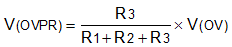
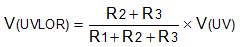
The undervoltage lockout (UVLO) and overvoltage trip point are adjusted using an external voltage divider network of R1, R2 and R3 connected between IN_SYS, UVLO, OVP and GND pins of the device. The values required for setting the undervoltage and overvoltage are calculated by solving Equation 9 and Equation 10.
For minimizing the input current drawn from the power supply {I(R123) = V(IN) / (R1 + R2 + R3)}, it is recommended to use higher value resistance for R1, R2 and R3.
However, the leakage current due to external active components connected at resistor string can add error to these calculations. So, the resistor string current, I(R123) must be chosen to be 20x greater than the leakage current of UVLO and OVP pins.
From the device electrical specifications, V(OVPR) = 1.2 V and V(UVLOR) = 1.2 V. From the design requirements, V(OV) is 33 V and V(UV) is 18 V. To solve the equation, first choose the value of R3 = 34 kΩ and use Equation 9 to solve for (R1 + R2) = 916 kΩ. Use Equation 10 and value of (R1 + R2) to solve for R2 = 29.4 kΩ and finally R1= 887 kΩ.
Choose the closest standard 1% resistor values: R1 = 887 kΩ, R2 = 29.4 kΩ, and R3 = 34 kΩ.
The UVLO and the OVP pins can also be connected to the GND pin to enable the internal default V(OV) = 34.2 V and V(UV) = 15.6 V.