SBVS300A November   2016  – September 2021 TPS3851

PRODUCTION DATA  

  1. Features
  2. Applications
  3. Description
  4. Revision History
  5. Pin Configuration and Functions
  6. Specifications
    1. 6.1 Absolute Maximum Ratings
    2. 6.2 ESD Ratings
    3. 6.3 Recommended Operating Conditions
    4. 6.4 Thermal Information
    5. 6.5 Electrical Characteristics
    6. 6.6 Timing Requirements
    7. 6.7 Timing Diagrams
    8. 6.8 Typical Characteristics
  7. Detailed Description
    1. 7.1 Overview
    2. 7.2 Functional Block Diagram
    3. 7.3 Feature Description
      1. 7.3.1 RESET
      2. 7.3.2 Manual Reset MR
      3. 7.3.3 UV Fault Detection
      4. 7.3.4 Watchdog Mode
        1. 7.3.4.1 CWD
        2. 7.3.4.2 Watchdog Input WDI
        3. 7.3.4.3 Watchdog Output WDO
        4. 7.3.4.4 SET1
    4. 7.4 Device Functional Modes
      1. 7.4.1 VDD is Below VPOR ( VDD < VPOR)
      2. 7.4.2 Above Power-On-Reset, But Less Than VDD(min) (VPOR ≤ VDD < VDD(min))
      3. 7.4.3 Normal Operation (VDD ≥ VDD(min))
  8. Application and Implementation
    1. 8.1 Application Information
      1. 8.1.1 CWD Functionality
        1. 8.1.1.1 Factory-Programmed Timing Options
        2. 8.1.1.2 Adjustable Capacitor Timing
      2. 8.1.2 Overdrive Voltage
    2. 8.2 Typical Application
      1. 8.2.1 Design Requirements
      2. 8.2.2 Detailed Design Procedure
        1. 8.2.2.1 Monitoring the 1.8-V Rail
        2. 8.2.2.2 Calculating RESET and WDO Pullup Resistor
        3. 8.2.2.3 Setting the Watchdog
        4. 8.2.2.4 Watchdog Disabled During Initialization Period
      3. 8.2.3 Glitch Immunity
      4. 8.2.4 Application Curves
  9. Power Supply Recommendations
  10. 10Layout
    1. 10.1 Layout Guidelines
    2. 10.2 Layout Example
  11. 11Device and Documentation Support
    1. 11.1 Device Support
      1. 11.1.1 Device Nomenclature
    2. 11.2 Documentation Support
      1. 11.2.1 Related Documentation
    3. 11.3 Receiving Notification of Documentation Updates
    4. 11.4 Support Resources
    5. 11.5 Trademarks
    6. 11.6 Electrostatic Discharge Caution
    7. 11.7 Glossary
  12. 12Mechanical, Packaging, and Orderable Information

Package Options

Mechanical Data (Package|Pins)
Thermal pad, mechanical data (Package|Pins)
Orderable Information

Description

The TPS3851 combines a precision voltage supervisor with a programmable watchdog timer. The TPS3851 comparator achieves a 0.8% accuracy
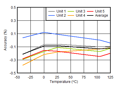
(–40°C to +125°C) for the undervoltage (VITN) threshold on the VDD pin. The TPS3851 also includes accurate hysteresis on the undervoltage threshold making the device ideal for use with tight tolerance systems. The supervisor RESET delay features a 15% accuracy, high-precision delay timing.

The TPS3851 includes a programmable watchdog timer for a wide variety of applications. The dedicated watchdog output (WDO) enables increased resolution to help determine the nature of fault conditions. The watchdog timeouts can be programmed either by an external capacitor, or by factory-programmed default delay settings. The watchdog can be disabled via logic pins to avoid undesired watchdog timeouts during the development process.

TPS3851 is available in a small 3.00-mm × 3.00-mm, 8-pin VSON package.

Device Information
PART NUMBER PACKAGE (1) BODY SIZE (NOM)
TPS3851 VSON (8) 3.00 mm × 3.00 mm
For all available packages, see the orderable addendum at the end of the data sheet.
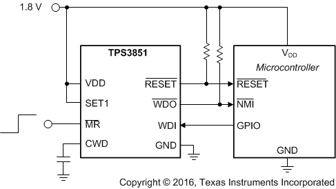
GUID-E15FD24A-2AE7-44D6-A29A-08D5C581CC30-low.gifFully Integrated Microcontroller Supervisory Circuit
GUID-98A16D2E-6E03-43AB-9647-9F017EDE04D7-low.gifUndervoltage Threshold (VITN) Accuracy vs Temperature