SLUS719H MARCH   2007  – May 2019 TPS40192 , TPS40193

PRODUCTION DATA.  

  1. Features
  2. Applications
  3. Description
    1.     Device Images
      1.      Simplified Application Diagram
  4. Revision History
  5. Pin Configuration and Functions
    1.     Pin Functions
  6. Specifications
    1. 6.1 Absolute Maximum Ratings
    2. 6.2 ESD Ratings
    3. 6.3 Recommended Operating Conditions
    4. 6.4 Thermal Information
    5. 6.5 Electrical Characteristics
    6. 6.6 Dissipation Ratings
    7. 6.7 Typical Characteristics
  7. Detailed Description
    1. 7.1 Overview
    2. 7.2 Functional Block Diagram
    3. 7.3 Feature Description
      1. 7.3.1  Voltage Reference
      2. 7.3.2  Oscillator
      3. 7.3.3  UVLO
      4. 7.3.4  Enable Functionality
      5. 7.3.5  Start-Up Sequence and Timing
      6. 7.3.6  Selecting the Short Circuit Current
      7. 7.3.7  5-V Regulator
      8. 7.3.8  Prebias Start-Up
      9. 7.3.9  Drivers
      10. 7.3.10 Power Good
      11. 7.3.11 Thermal Shutdown
    4. 7.4 Device Functional Modes
      1. 7.4.1 Continuous Conduction Mode
      2. 7.4.2 Low-Quiescent Shutdown
  8. Application and Implementation
    1. 8.1 Application Information
    2. 8.2 Typical Application
      1. 8.2.1 Design Requirements
      2. 8.2.2 Detailed Design Procedure
        1. 8.2.2.1  Selecting the Switching Frequency
        2. 8.2.2.2  Inductor Selection
        3. 8.2.2.3  Output Capacitor Selection (C8)
        4. 8.2.2.4  Peak Current Rating of the Inductor
        5. 8.2.2.5  Input Capacitor Selection (C7)
        6. 8.2.2.6  MOSFET Switch Selection (Q1, Q2)
        7. 8.2.2.7  Boot Strap Capacitor
        8. 8.2.2.8  Input Bypass Capacitor (C6)
        9. 8.2.2.9  BP5 Bypass Capacitor (C5)
        10. 8.2.2.10 Input Voltage Filter Resistor (R11)
        11. 8.2.2.11 Short Circuit Protection (R9)
        12. 8.2.2.12 Feedback Compensation (Modeling the Power Stage)
        13. 8.2.2.13 Feedback Divider (R7, R8)
        14. 8.2.2.14 Error Amplifier Compensation (R6, R10, C1, C2, C3)
      3. 8.2.3 Application Curves
  9. Power Supply Recommendations
  10. 10Layout
    1. 10.1 Layout Guidelines
    2. 10.2 Layout Examples
  11. 11Device and Documentation Support
    1. 11.1 Device Support
      1. 11.1.1 Development Support
        1. 11.1.1.1 Related Devices
      2. 11.1.2 Device Nomenclature
    2. 11.2 Documentation Support
    3. 11.3 Related Links
    4. 11.4 Receiving Notification of Documentation Updates
    5. 11.5 Community Resources
    6. 11.6 Trademarks
    7. 11.7 Electrostatic Discharge Caution
    8. 11.8 Glossary
  12. 12Mechanical, Packaging, and Orderable Information

Package Options

Mechanical Data (Package|Pins)
Thermal pad, mechanical data (Package|Pins)
Orderable Information

Typical Application

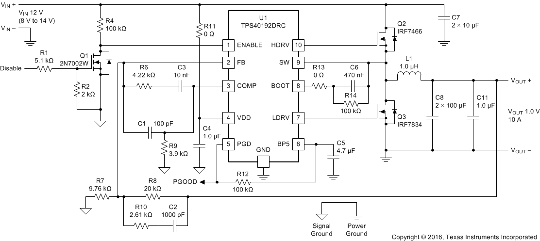
TPS40192 TPS40193 v13106_lus719.gifFigure 15. TPS40192 Design Example Schematic