SLUS600E April 2004 – December 2014 TPS51100
PRODUCTION DATA.
- 1 Features
- 2 Applications
- 3 Description
- 4 Revision History
- 5 Pin Configuration and Functions
- 6 Specifications
- 7 Detailed Description
- 8 Application and Implementation
- 9 Power Supply Recommendations
- 10Layout
- 11Device and Documentation Support
- 12Mechanical, Packaging, and Orderable Information
Package Options
Refer to the PDF data sheet for device specific package drawings
Mechanical Data (Package|Pins)
- DGQ|10
Thermal pad, mechanical data (Package|Pins)
- DGQ|10
Orderable Information
7 Detailed Description
7.1 Overview
The TPS51100 is a sink / source double date rate (DDR) termination regulator with VTTREF buffered reference output.
7.2 Functional Block Diagram
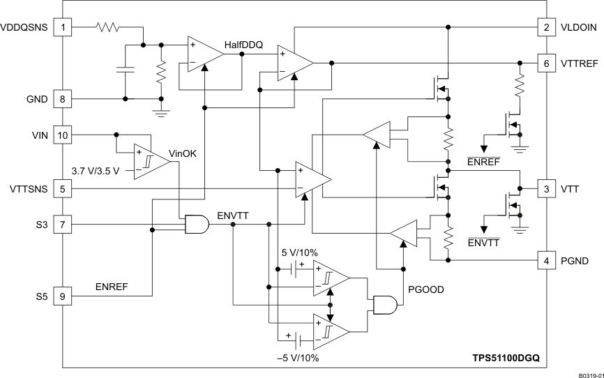 Figure 22. Simplified Block Diagram
7.3 Feature Description
7.3.1 VTT Sink/Source Regulator
The TPS51100 is a 3-A sink/source tracking termination regulator designed specially for low-cost, low-external-components systems where space is at premium, such as notebook PC applications. The TPS51100 integrates a high-performance, low-dropout linear regulator that is capable of sourcing and sinking current up to 3 A. This VTT linear regulator employs an ultimate fast-response feedback loop so that small ceramic capacitors are enough to keep tracking to the VTTREF within ±40 mV under all conditions, including fast load transient. To achieve tight regulation with minimum effect of trace resistance, a remote sensing terminal, VTTSNS, should be connected to the positive node of the VTT output capacitor(s) as a separate trace from the high-current line from VTT.
7.3.2 VTTREF Regulator
The VTTREF block consists of an on-chip 1/2 divider, low-pass filter (LPF), and buffer. This regulator can source current up to 10 mA. Bypass VTTREF to GND using a 0.1-μF ceramic capacitor to ensure stable operation.
7.3.3 Soft-Start
The soft-start function of the VTT is achieved via a current clamp, allowing the output capacitors to be charged with low and constant current that gives linear ramp-up of the output voltage. The current-limit threshold is changed in two stages using an internal powergood signal. When VTT is outside the powergood threshold, the current limit level is 2.2 A. When VTT rises above (VTTREF – 5%) or falls below (VTTREF + 5%), the current limit level switches to 3.8 A. The thresholds are typically VTTREF ±5% (from outside regulation to inside) and ±10% (when it falls outside). The soft-start function is completely symmetrical, and it works not only from GND to VTTREF voltage, but also from VDDQ to VTTREF voltage. Note that the VTT output is in a high-impedance state during the S3 state (S3 = low, S5 = high), and its voltage can be up to VDDQ voltage, depending on the external condition. Note that VTT does not start under a full-load condition.
7.3.4 VTT Current Protection
The LDO has a constant overcurrent limit (OCL) at 3.8 A. This trip point is reduced to 2.2 A before the output voltage comes within ±5% of the target voltage or goes outside of ±10% of the target voltage.
7.3.5 VIN UVLO Protection
For VIN undervoltage lockout (UVLO) protection, the TPS51100 monitors VIN voltage. When the VIN voltage is lower than UVLO threshold voltage, the VTT regulator is shut off. This is a non-latch protection.
7.3.6 Thermal Shutdown
TPS51100 monitors its temperature. If the temperature exceeds the threshold value, typically 160°C, the VTT and VTTREF regulators are shut off. This is also a non-latch protection.
7.4 Device Functional Modes
7.4.1 S5 Control and Soft-Off
The S3 and S5 terminals should be connected to SLP_S3 and SLP_S5 signals, respectively. Both VTTREF and VTT are turned on at the S0 state (S3 = high, S5 = high). VTTREF is kept alive while VTT is turned off and left high-impedance in the S3 state (S3 = low, S5 = high). Both VTT and VTTREF outputs are turned off and discharged to ground through internal MOSFETs during S4/S5 state (both S3 and S5 are low).