SLUS600E April 2004 – December 2014 TPS51100
PRODUCTION DATA.
- 1 Features
- 2 Applications
- 3 Description
- 4 Revision History
- 5 Pin Configuration and Functions
- 6 Specifications
- 7 Detailed Description
- 8 Application and Implementation
- 9 Power Supply Recommendations
- 10Layout
- 11Device and Documentation Support
- 12Mechanical, Packaging, and Orderable Information
Package Options
Refer to the PDF data sheet for device specific package drawings
Mechanical Data (Package|Pins)
- DGQ|10
Thermal pad, mechanical data (Package|Pins)
- DGQ|10
Orderable Information
6 Specifications
6.1 Absolute Maximum Ratings
over operating free-air temperature range (unless otherwise noted)(1)| MIN | MAX | UNIT | |||
|---|---|---|---|---|---|
| Input voltage(2) | VIN, VLDOIN, VTTSNS, VDDQSNS, S3, S5 | –0.3 | 6 | V | |
| PGND | –0.3 | 0.3 | |||
| Output voltage(2) | VTT, VTTREF | –0.3 | 6 | V | |
| TA | Operating ambient temperature | –40 | 85 | °C | |
| Tstg | Storage temperature | –55 | 150 | °C | |
(1) Stresses beyond those listed under Absolute Maximum Ratings may cause permanent damage to the device. These are stress ratings only, and functional operation of the device at these or any other conditions beyond those indicated under RecommendedOperating Conditions is not implied. Exposure to absolute-maximum-rated conditions for extended periods may affect device reliability.
(2) All voltage values are with respect to the network ground terminal unless otherwise noted.
6.2 Recommended Operating Conditions
over operating free-air temperature range (unless otherwise noted)| MIN | MAX | UNIT | |||
|---|---|---|---|---|---|
| VIN | Supply voltage | 4.75 | 5.25 | V | |
| Voltage range | S3, S5 | –0.10 | 5.25 | V | |
| VLDOIN, VDDQSNS, VTT, VTTSNS | –0.1 | 3.6 | |||
| VTTREF | –0.1 | 1.8 | |||
| PGND | –0.1 | 0.1 | |||
| TA | Operating free-air temperature | –40 | 85 | °C | |
6.3 Thermal Information
| THERMAL METRIC(1) | TPS51100 | UNIT | ||
|---|---|---|---|---|
| DGQ | ||||
| 10 PINS | ||||
| RθJA | Junction-to-ambient thermal resistance | 60.3 | °C/W | |
| RθJC(top) | Junction-to-case (top) thermal resistance | 63.5 | ||
| RθJB | Junction-to-board thermal resistance | 51.6 | ||
| ψJT | Junction-to-top characterization parameter | 1.5 | ||
| ψJB | Junction-to-board characterization parameter | 22.3 | ||
| RθJC(bot) | Junction-to-case (bottom) thermal resistance | 9.5 | ||
(1) For more information about traditional and new thermal metrics, see the IC Package Thermal Metrics application report, SPRA953.
6.4 Electrical Characteristics
TA = –40°C to 85°C, VVIN = 5 V, VLDOIN and VDDQSNS are connected to 2.5 V (unless otherwise noted)| PARAMETER | TEST CONDITIONS | MIN | TYP | MAX | UNIT | |||
|---|---|---|---|---|---|---|---|---|
| SUPPLY CURRENT | ||||||||
| IVIN | Supply current, VIN | TA = 25°C, VVIN = 5 V, no load, VS3 = VS5 = 5 V | 0.25 | 0.5 | 1 | mA | ||
| IVINSTB | Standby currrent, VIN | TA = 25°C, VVIN = 5 V, no load, VS3 = 0 V, VS5 = 5 V | 25 | 50 | 80 | μA | ||
| IVINSDN | Shutdown current, VIN | TA = 25°C, VVIN = 5 V, no load, VS3 = VS5 = 0 V, VVLDOIN = VVDDQSNS = 0 V | 0.3 | 1 | μA | |||
| IVLDOIN | Supply current, VLDOIN | TA = 25°C, VVIN = 5 V, no load, VS3 = VS5 = 5 V | 0.7 | 1.2 | 2 | mA | ||
| IVLDOINSTB | Standby currrent, VLDOIN | TA = 25°C, VVIN = 5 V, no load,VS3 = 0 V, VS5 = 5 V | 6 | 10 | μA | |||
| IVLDOINSDN | Shutdown current, VLDOIN | TA = 25°C, VVIN = 5 V, no load, VS3 = VS5 = 0 V | 0.3 | 1 | μA | |||
| INPUT CURRENT | ||||||||
| IVDDQSNS | Input current, VDDQSNS | VVIN = 5 V, VS3 = VS5 = 5 V | 1 | 3 | 5 | μA | ||
| IVTTSNS | Input current, VTTSNS | VVIN = 5 V, VS3 = VS5 = 5 V | –1 | –0.25 | 1 | μA | ||
| VTT OUTPUT | ||||||||
| VVTTSNS | Output voltage, VTT | VVLDOIN = VVDDQSNS = 2.5 V | 1.25 | V | ||||
| VVLDOIN = VVDDQSNS = 1.8 V | 0.9 | |||||||
| VVLDOIN = VVDDQSNS = 1.5 V | 0.75 | |||||||
| VVTTTOL25 | Output votlage tolerance to VTTREF, VTT | VVLDOIN = VVDDQSNS = 2.5 V, |IVTT| = 0 A | –20 | 20 | mV | |||
| VVLDOIN = VVDDQSNS = 2.5 V, |IVTT| = 1.5 A | –30 | 30 | ||||||
| VVLDOIN = VVDDQSNS = 2.5 V, |IVTT| = 3 A | –40 | 40 | ||||||
| VVTTTOL18 | VVLDOIN = VVDDQSNS = 1.8 V, |IVTT| = 0 A | –20 | 20 | |||||
| VVLDOIN = VVDDQSNS = 1.8 V, |IVTT| = 1 A | –30 | 30 | ||||||
| VVLDOIN = VVDDQSNS = 1.8 V, |IVTT| = 2 A | –40 | 40 | ||||||
| VVTTTOL15 | VVLDOIN = VVDDQSNS = 1.5 V, |IVTT| = 0 A | –20 | 20 | |||||
| VVLDOIN = VVDDQSNS = 1.5 V, |IVTT| = 1 A | –30 | 30 | ||||||
| IVTTOCLSRC | Source current limit, VTT | 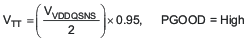 |
3 | 3.8 | 6 | A | ||
| VVTT = 0 V | 1.5 | 2.2 | 3 | |||||
| IVTTOCLSNK | Sink current limit, VTT | 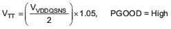 |
3 | 3.6 | 6 | A | ||
| VVTT = VVDDQ | 1.5 | 2.2 | 3 | |||||
| IVTTLK | Leakage current, VTT | 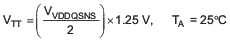 |
–1 | 0.5 | 10 | μA | ||
| VS3 = 0 V, | VS5 = 5 V | |||||||
| IVTTSNSLK | Leakage current, VTTSNS | |
–1 | 0.01 | 1 | μA | ||
| IDSCHRG | Discharge current, VTT | TA = 25°C, VVDDQSNS = 0 V, |
VS3 = VS5 = 0 V, VVTT = 0.5 V |
10 | 17 | mA | ||
| VTTREF OUTPUT | ||||||||
| VVTTREF | Output voltage, VTTREF |  |
V | |||||
| VVTTREFTOL25 | Output voltage tolerance to VDDQSNS/2, VTTREF | VVLDOIN = VVDDQSNS = 2.5 V, IVTTREF < 10 mA | –20 | 20 | mV | |||
| VVTTREFTOL18 | VVLDOIN = VVDDQSNS = 1.8 V, IVTTREF < 10 mA | –17 | 17 | |||||
| VVTTREFTOL15 | VVLDOIN = VVDDQSNS = 1.5 V, IVTTREF < 10 mA | –15 | 15 | |||||
| IVTTREFOCL | Source current limit, VTTREF | VVTTREF = 0 V | 10 | 20 | 30 | mA | ||
| UVLO/LOGIC THRESHOLD | ||||||||
| VVINUV | UVLO threshold voltage, VIN | Wake up | 3.4 | 3.7 | 4 | V | ||
| Hysteresis | 0.15 | 0.25 | 0.35 | |||||
| VIH | High-level input voltage | S3, S5 | 1.6 | V | ||||
| VIL | Low-level input voltage | S3, S5 | 0.3 | V | ||||
| VIHYST | Hysteresis voltage | S3, S5 | 0.2 | V | ||||
| IILEAK | Logic input leakage current | S2, S5, | TA = 25°C | –1 | 1 | μA | ||
| THERMAL SHUTDOWN | ||||||||
| TSDN | Thermal shutdown threshold | Shutdown temperature | 160 | °C | ||||
| Hysteresis | 10 | |||||||
6.5 Typical Characteristics
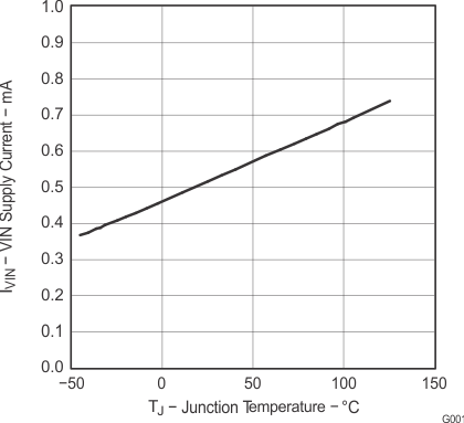 Figure 1. VIN Supply Current vs Temperature
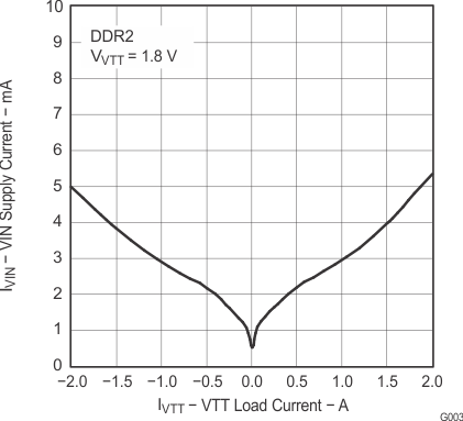 Figure 3. VIN Supply Current vs VTT Load Current
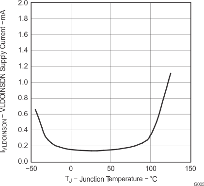 Figure 5. VLDOIN Shutdown Current vs Temperature
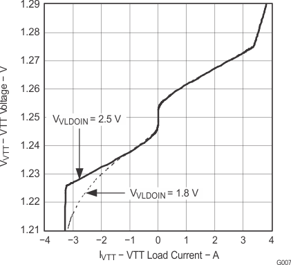 Figure 7. VTT Voltage Load Regulation vs VTT Load Current (DDR)
 Figure 9. VTT Voltage Load Regulation vs VTT Load Current (DDR3)
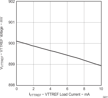 Figure 11. VTTREF Voltage Load Regulation vs VTTREF Load Current (DDR2)
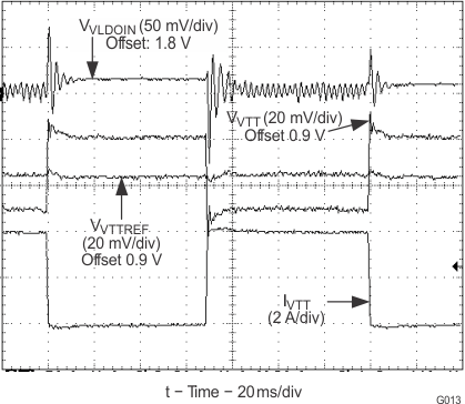 Figure 13. VTT Voltage Load Transient Response
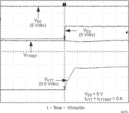 Figure 15. Startup Waveforms S3 Low-to-High
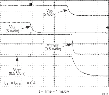 Figure 17. Shutdown Waveforms S3 and S5 High-to-Low
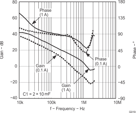 Figure 19. Bode Plot DDR Sink
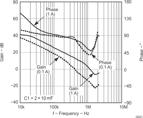 Figure 21. Bode Plot DDR2 Sink
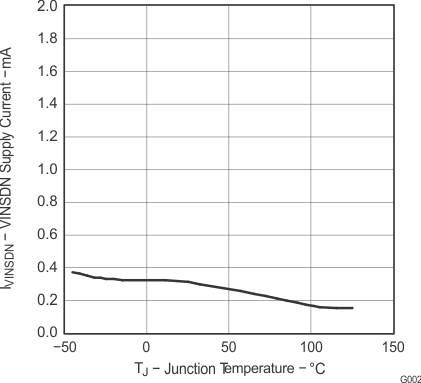 Figure 2. VIN Shutdown Current vs Temperature
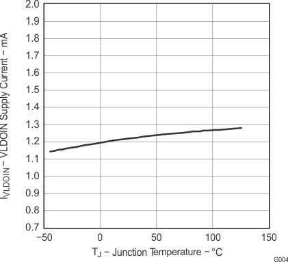 Figure 4. VLDOIN Supply Current vs Temperature
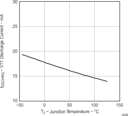 Figure 6. Discharge Current vs Temperature
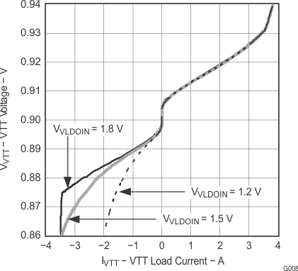 Figure 8. VTT Voltage Load Regulation vs VTT Load Current (DDR2)
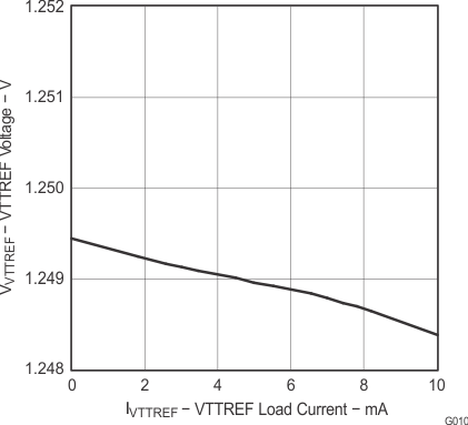 Figure 10. VTTREF Voltage Load Regulation vs VTTREF Load Current (DDR)
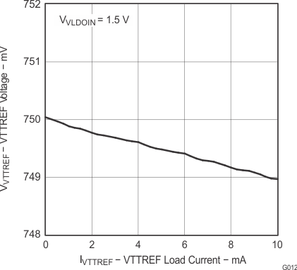 Figure 12. VTTREF Voltage Load Regulation vs VTTREF Load Current (DDR3)
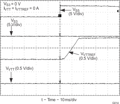 Figure 14. Startup Waveforms S5 Low-to-High
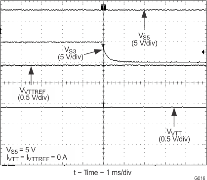 Figure 16. Shutdown Waveforms S3 High-to-Low
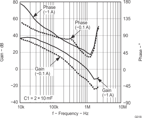 Figure 18. Bode Plot DDR Source
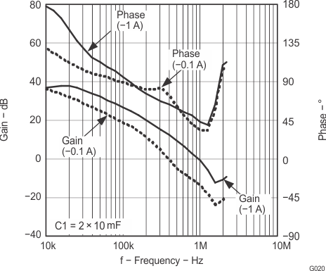 Figure 20. Bode Plot DDR2 Source