SLUS600E April 2004 – December 2014 TPS51100
PRODUCTION DATA.
- 1 Features
- 2 Applications
- 3 Description
- 4 Revision History
- 5 Pin Configuration and Functions
- 6 Specifications
- 7 Detailed Description
- 8 Application and Implementation
- 9 Power Supply Recommendations
- 10Layout
- 11Device and Documentation Support
- 12Mechanical, Packaging, and Orderable Information
Package Options
Refer to the PDF data sheet for device specific package drawings
Mechanical Data (Package|Pins)
- DGQ|10
Thermal pad, mechanical data (Package|Pins)
- DGQ|10
Orderable Information
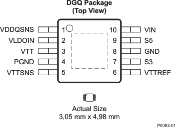
5 Pin Configuration and Functions
For more information on the DGQ package, see the PowerPAD Thermally Enhanced Package application report (SLMA002).
Pin Functions
| PIN | I/O | DESCRIPTION | |
|---|---|---|---|
| NAME | NO. | ||
| GND | 8 | – | Signal ground. Connect to negative terminal of the output capacitor |
| PGND | 4 | – | Power ground output for the VTT LDO |
| S3 | 7 | I | S3 signal input |
| S5 | 9 | I | S5 signal input |
| VDDQSNS | 1 | I | VDDQ sense input |
| VIN | 10 | I | 5-V power supply |
| VLDOIN | 2 | I | Power supply for the VTT LDO and VTTREF output stage |
| VTT | 3 | O | Power output for the VTT LDO |
| VTTREF | 6 | O | VTT reference output. Connect to GND through 0.1-μF ceramic capacitor. |
| VTTSNS | 5 | I | Voltage sense input for the VTT LDO. Connect to plus terminal of the output capacitor. |