SLVSB10F July 2012 – November 2020 TPS54020
PRODUCTION DATA
- 1 Features
- 2 Applications
- 3 Description
- 4 Revision History
- 5 Description (Continued)
- 6 Pin Configuration and Functions
- 7 Specifications
-
8 Detailed Description
- 8.1 Overview
- 8.2 Functional Block Diagram
- 8.3
Feature Description
- 8.3.1 Fixed Frequency PWM Control
- 8.3.2 Input Voltage and Power Input Voltage Pins (VIN and PVIN)
- 8.3.3 Voltage Reference (VREF)
- 8.3.4 Adjusting the Output Voltage
- 8.3.5 Safe Start-up into Prebiased Outputs
- 8.3.6 Error Amplifier
- 8.3.7 Slope Compensation
- 8.3.8 Enable and Adjusting Undervoltage Lockout
- 8.3.9 Adjustable Switching Frequency and Synchronization (RT/CLK)
- 8.3.10 Soft-Start (SS) Sequence
- 8.3.11 Power Good (PWRGD)
- 8.3.12 Bootstrap Voltage (BOOT) and Low Dropout Operation
- 8.3.13 Sequencing (SS)
- 8.3.14 Output Overvoltage Protection (OVP)
- 8.3.15 Overcurrent Protection
- 8.3.16 Thermal Shutdown
- 8.4 Device Functional Modes
-
9 Application and Implementation
- 9.1 Application Information
- 9.2
Typical Application
- 9.2.1 Design Requirements
- 9.2.2
Detailed Design Procedure
- 9.2.2.1 Custom Design With WEBENCH® Tools
- 9.2.2.2 Operating Frequency
- 9.2.2.3 Output Inductor Selection
- 9.2.2.4 Output Capacitor Selection
- 9.2.2.5 Input Capacitor Selection
- 9.2.2.6 Soft-Start Capacitor Selection
- 9.2.2.7 Bootstrap Capacitor Selection
- 9.2.2.8 Undervoltage Lockout Set Point
- 9.2.2.9 Output Voltage Feedback Resistor Selection
- 9.2.2.10 Compensation Component Selection
- 9.2.3 Application Curves
- 10Power Supply Recommendations
- 11Layout
- 12Device and Documentation Support
- 13Mechanical, Packaging, and Orderable Information
Package Options
Mechanical Data (Package|Pins)
- RUW|15
Thermal pad, mechanical data (Package|Pins)
- RUW|15
Orderable Information
6 Pin Configuration and Functions
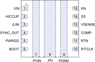
 Figure 6-1 15-Pin VQFNRUW Package(Top View)
Table 6-1 Pin Functions
| PIN | I/O(1) | DESCRIPTION | |
|---|---|---|---|
| NAME | NO. | ||
| BOOT | 6 | S | A bootstrap capacitor is required between BOOT and PH. If the voltage on this capacitor is below the minimum required by the high-side MOSFET (BOOT UVLO), the PH node is forced low so that the capacitor is refreshed. |
| COMP | 12 | O | Error amplifier current output, and input to the output switch current comparator. Connect frequency compensation to this pin. |
| EN | 15 | I | A divider network must be used to implement an undervoltage lockout function. To disable switching and reduce quiescent current, this pin must be pulled to ground. |
| HICCUP | 2 | O | Overcurrent protection scheme select pin |
| ILIM | 3 | O | Current limit threshold select pin |
| PGND | 9 | G | Power Ground. Return for the low-side MOSFET |
| PH | 8 | O | Switch node |
| PVIN | 7 | I | Power input. Supplies the power switches of the power converter |
| PWRGD | 5 | O | Power-good fault pin. Asserts low if output voltage is out of regulation due to thermal shutdown, dropout, overvoltage, EN shutdown, or during soft start. |
| RT/CLK | 10 | I/O | Automatically selects between RT mode and CLK mode. An external timing resistor adjusts the switching frequency of the device. In CLK mode, the device synchronizes to an external clock. |
| RTN | 11 | G | Return for control circuitry |
| SS | 14 | I/O | Soft-start pin. An external capacitor connected to this pin sets the internal voltage reference rise time. The voltage on this pin overrides the internal reference. It can be used for sequencing. |
| SYNC_OUT | 4 | O | Synchronization output provides a clock signal 180° out-of-phase with the power switch. |
| VIN | 1 | I | Supplies the control circuitry of the power converter |
| VSENSE | 13 | I | Inverting node of the transconductance (gm) error amplifier |
(1) I = Input, O = Output, S = Supply, G = Ground Return