SLVSB10F July 2012 – November 2020 TPS54020
PRODUCTION DATA
- 1 Features
- 2 Applications
- 3 Description
- 4 Revision History
- 5 Description (Continued)
- 6 Pin Configuration and Functions
- 7 Specifications
-
8 Detailed Description
- 8.1 Overview
- 8.2 Functional Block Diagram
- 8.3
Feature Description
- 8.3.1 Fixed Frequency PWM Control
- 8.3.2 Input Voltage and Power Input Voltage Pins (VIN and PVIN)
- 8.3.3 Voltage Reference (VREF)
- 8.3.4 Adjusting the Output Voltage
- 8.3.5 Safe Start-up into Prebiased Outputs
- 8.3.6 Error Amplifier
- 8.3.7 Slope Compensation
- 8.3.8 Enable and Adjusting Undervoltage Lockout
- 8.3.9 Adjustable Switching Frequency and Synchronization (RT/CLK)
- 8.3.10 Soft-Start (SS) Sequence
- 8.3.11 Power Good (PWRGD)
- 8.3.12 Bootstrap Voltage (BOOT) and Low Dropout Operation
- 8.3.13 Sequencing (SS)
- 8.3.14 Output Overvoltage Protection (OVP)
- 8.3.15 Overcurrent Protection
- 8.3.16 Thermal Shutdown
- 8.4 Device Functional Modes
-
9 Application and Implementation
- 9.1 Application Information
- 9.2
Typical Application
- 9.2.1 Design Requirements
- 9.2.2
Detailed Design Procedure
- 9.2.2.1 Custom Design With WEBENCH® Tools
- 9.2.2.2 Operating Frequency
- 9.2.2.3 Output Inductor Selection
- 9.2.2.4 Output Capacitor Selection
- 9.2.2.5 Input Capacitor Selection
- 9.2.2.6 Soft-Start Capacitor Selection
- 9.2.2.7 Bootstrap Capacitor Selection
- 9.2.2.8 Undervoltage Lockout Set Point
- 9.2.2.9 Output Voltage Feedback Resistor Selection
- 9.2.2.10 Compensation Component Selection
- 9.2.3 Application Curves
- 10Power Supply Recommendations
- 11Layout
- 12Device and Documentation Support
- 13Mechanical, Packaging, and Orderable Information
Package Options
Mechanical Data (Package|Pins)
- RUW|15
Thermal pad, mechanical data (Package|Pins)
- RUW|15
Orderable Information
9.2.2.3 Output Inductor Selection
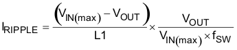
To calculate the value of the output inductor, use Equation 18. KIND is a coefficient that represents the amount of inductor ripple current relative to the maximum output current. The inductor ripple current is filtered by the output capacitor. Therefore, choosing high inductor ripple currents impact the selection of the output capacitor because the output capacitor must have a ripple current rating equal to or greater than the inductor ripple current. In general, the inductor ripple value is at the discretion of the designer; however, KIND is normally from 0.1 to 0.3 for the majority of applications.
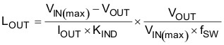
For this design example, use KIND = 0.3 and the inductor value is calculated to be 1.07 μH. For this design, a nearest standard value was chosen at 1 μH. For the output filter inductor, it is important that the rms current and saturation current ratings not be exceeded. The rms and peak inductor current are calculated in Equation 19 and Equation 20.
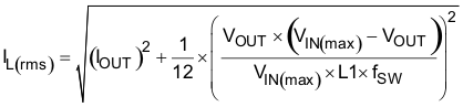
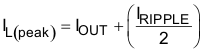
For this design, the rms inductor current is calculated to be 10.04 A and the peak inductor current is 11.6 A.
The chosen inductor is 1.0 μH, with a saturation current rating of 13 A. The current flowing through the inductor is the inductor ripple current plus the output current. During power up, faults, or transient load conditions, the inductor current can increase above the peak inductor current level calculated above. In transient conditions, the inductor current can increase up to the switch current limit of the device. For this reason, the most conservative approach is to specify an inductor with a saturation current rating equal to or greater than the switch current limit rather than the peak inductor current.