SLVSB10F July 2012 – November 2020 TPS54020
PRODUCTION DATA
- 1 Features
- 2 Applications
- 3 Description
- 4 Revision History
- 5 Description (Continued)
- 6 Pin Configuration and Functions
- 7 Specifications
-
8 Detailed Description
- 8.1 Overview
- 8.2 Functional Block Diagram
- 8.3
Feature Description
- 8.3.1 Fixed Frequency PWM Control
- 8.3.2 Input Voltage and Power Input Voltage Pins (VIN and PVIN)
- 8.3.3 Voltage Reference (VREF)
- 8.3.4 Adjusting the Output Voltage
- 8.3.5 Safe Start-up into Prebiased Outputs
- 8.3.6 Error Amplifier
- 8.3.7 Slope Compensation
- 8.3.8 Enable and Adjusting Undervoltage Lockout
- 8.3.9 Adjustable Switching Frequency and Synchronization (RT/CLK)
- 8.3.10 Soft-Start (SS) Sequence
- 8.3.11 Power Good (PWRGD)
- 8.3.12 Bootstrap Voltage (BOOT) and Low Dropout Operation
- 8.3.13 Sequencing (SS)
- 8.3.14 Output Overvoltage Protection (OVP)
- 8.3.15 Overcurrent Protection
- 8.3.16 Thermal Shutdown
- 8.4 Device Functional Modes
-
9 Application and Implementation
- 9.1 Application Information
- 9.2
Typical Application
- 9.2.1 Design Requirements
- 9.2.2
Detailed Design Procedure
- 9.2.2.1 Custom Design With WEBENCH® Tools
- 9.2.2.2 Operating Frequency
- 9.2.2.3 Output Inductor Selection
- 9.2.2.4 Output Capacitor Selection
- 9.2.2.5 Input Capacitor Selection
- 9.2.2.6 Soft-Start Capacitor Selection
- 9.2.2.7 Bootstrap Capacitor Selection
- 9.2.2.8 Undervoltage Lockout Set Point
- 9.2.2.9 Output Voltage Feedback Resistor Selection
- 9.2.2.10 Compensation Component Selection
- 9.2.3 Application Curves
- 10Power Supply Recommendations
- 11Layout
- 12Device and Documentation Support
- 13Mechanical, Packaging, and Orderable Information
Package Options
Mechanical Data (Package|Pins)
- RUW|15
Thermal pad, mechanical data (Package|Pins)
- RUW|15
Orderable Information
9.2.2.6 Soft-Start Capacitor Selection
The soft-start capacitor determines the minimum amount of time it takes for the output voltage to reach its nominal programmed value during power up. This is useful if a load requires a controlled voltage slew rate. This is also used if the output capacitance is very large and would require large amounts of current to quickly charge the capacitor to the output voltage level. The extra current required to charge the output capacitors can cause the TPS54020 to reach the current limit. The soft-start current surge from the input can cause the input voltage rail to sag. Limiting the output voltage slew rate solves both of these problems. The soft-start capacitor value can be calculated using Equation 28. For the example circuit, the soft-start time is not critical because the output capacitor value is only 300 μF which does not require much current to charge to 1.8 V. The example circuit has the soft-start time set to an arbitrary value of 30 ms, which requires a 100-nF capacitor. In this case, ISS is 2.3 µA and VREF is 0.6 V.
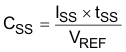
where
- CSS is the soft-start capacitance in nF
- ISS is the soft-start current in µA
- tSS is the soft-start time in ms
- VREF of the voltage reference in V