SLVSD26B April 2016 – April 2021 TPS54202
PRODUCTION DATA
- 1 Features
- 2 Applications
- 3 Description
- 4 Revision History
- 5 Pin Configuration and Functions
- 6 Specifications
-
7 Detailed Description
- 7.1 Overview
- 7.2 Functional Block Diagram
- 7.3
Feature Description
- 7.3.1 Fixed-Frequency PWM Control
- 7.3.2 Pulse Skip Mode
- 7.3.3 Error Amplifier
- 7.3.4 Slope Compensation and Output Current
- 7.3.5 Enable and Adjusting Under Voltage Lockout
- 7.3.6 Safe Startup into Pre-Biased Outputs
- 7.3.7 Voltage Reference
- 7.3.8 Adjusting Output Voltage
- 7.3.9 Internal Soft-Start
- 7.3.10 Bootstrap Voltage (BOOT)
- 7.3.11 Overcurrent Protection
- 7.3.12 Spread Spectrum
- 7.3.13 Output Overvoltage Protection (OVP)
- 7.3.14 Thermal Shutdown
- 7.4 Device Functional Modes
- 8 Application and Implementation
- 9 Power Supply Recommendations
- 10Layout
- 11Device and Documentation Support
- 12Mechanical, Packaging, and Orderable Information
Package Options
Mechanical Data (Package|Pins)
- DDC|6
Thermal pad, mechanical data (Package|Pins)
Orderable Information
3 Description
The TPS54202 is a 4.5-V to 28-V input voltage range, 2-A synchronous buck converter. The device includes two integrated switching FETs, internal loop compensation and 5-ms internal soft start to reduce component count.
By integrating the MOSFETs and employing the SOT-23 package, the TPS54202 achieves the high power density and offers a small footprint on the PCB.
Advanced Eco-mode implementation maximizes the light load efficiency and reduces the power loss.
The frequency spread spectrum operation is introduced for EMI reduction.
Cycle-by-cycle current limit in both high-side MOSFET protects the converter in an overload condition and is enhanced by a low-side MOSFET freewheeling current limit which prevents current runaway. Hiccup mode protection is triggered if the overcurrent condition has persisted for longer than the present time.
| PART NUMBER | PACKAGE(1) | BODY SIZE (NOM) |
|---|---|---|
| TPS54202 | SOT-23 (6) | 1.60 mm × 2.90 mm |
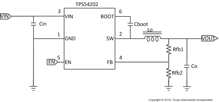
 Simplified Schematic
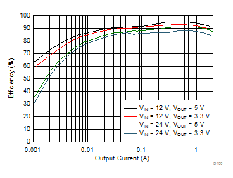
 Efficiency vs Output
Current