SLVSD26B April 2016 – April 2021 TPS54202
PRODUCTION DATA
- 1 Features
- 2 Applications
- 3 Description
- 4 Revision History
- 5 Pin Configuration and Functions
- 6 Specifications
-
7 Detailed Description
- 7.1 Overview
- 7.2 Functional Block Diagram
- 7.3
Feature Description
- 7.3.1 Fixed-Frequency PWM Control
- 7.3.2 Pulse Skip Mode
- 7.3.3 Error Amplifier
- 7.3.4 Slope Compensation and Output Current
- 7.3.5 Enable and Adjusting Under Voltage Lockout
- 7.3.6 Safe Startup into Pre-Biased Outputs
- 7.3.7 Voltage Reference
- 7.3.8 Adjusting Output Voltage
- 7.3.9 Internal Soft-Start
- 7.3.10 Bootstrap Voltage (BOOT)
- 7.3.11 Overcurrent Protection
- 7.3.12 Spread Spectrum
- 7.3.13 Output Overvoltage Protection (OVP)
- 7.3.14 Thermal Shutdown
- 7.4 Device Functional Modes
- 8 Application and Implementation
- 9 Power Supply Recommendations
- 10Layout
- 11Device and Documentation Support
- 12Mechanical, Packaging, and Orderable Information
Package Options
Mechanical Data (Package|Pins)
- DDC|6
Thermal pad, mechanical data (Package|Pins)
Orderable Information
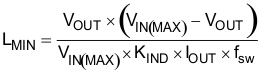
8.2.3.5.1 Inductor Selection
Use Equation 8 to calculate the minimum value of the output inductor (LMIN).
Where:
KIND is a coefficient that represents the amount of inductor ripple current relative to the maximum output current.
In general, the value of KIND is at the discretion of the designer; however, the following guidelines may be used. For designs using low-ESR output capacitors, such as ceramics, a value as high as KIND = 0.3 can be used. When using higher ESR output capacitors, KIND = 0.2 yields better results.
For this design example, use KIND = 0.3. The minimum inductor value is calculated as 13.7 μH. For this design, a close standard value of 15 μH was selected for LMIN.
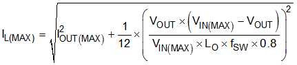
For the output filter inductor, the RMS current and saturation current ratings must not be exceeded. Use Equation 9 to calculate the RMS inductor current (IL(RMS)).
Use Equation 10 to calculate the peak inductor current (IL(PK)).
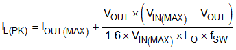
Smaller or larger inductor values can be used depending on the amount of ripple current the designer wants to allow so long as the other design requirements are met. Larger value inductors have lower AC current and result in lower output voltage ripple. Smaller inductor values increase AC current and output voltage ripple.