SLVSCG7A July 2014 – September 2021 TPS55340-EP
PRODUCTION DATA
- 1 Features
- 2 Applications
- 3 Description
- 4 Revision History
- 5 Description (continued)
- 6 Pin Configuration and Functions
- 7 Specifications
-
8 Detailed Description
- 8.1 Overview
- 8.2 Functional Block Diagram
- 8.3
Feature Description
- 8.3.1 Switching Frequency
- 8.3.2 Voltage Reference and Setting Output Voltage
- 8.3.3 Soft Start
- 8.3.4 Slope Compensation
- 8.3.5 Overcurrent Protection and Frequency Foldback
- 8.3.6 Enable and Thermal Shutdown
- 8.3.7 Undervoltage Lockout (UVLO)
- 8.3.8 Minimum On-Time and Pulse Skipping
- 8.3.9 Layout Considerations
- 8.3.10 Thermal Considerations
- 8.4 Device Functional Modes
-
9 Application and Implementation
- 9.1 Application Information
- 9.2
Typical Applications
- 9.2.1
Boost Converter Application
- 9.2.1.1 Design Requirements
- 9.2.1.2
Detailed Design Procedure
- 9.2.1.2.1 Selecting the Switching Frequency (R4)
- 9.2.1.2.2 Determining the Duty Cycle
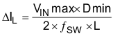
- 9.2.1.2.3 Selecting the Inductor (L1)
- 9.2.1.2.4 Computing the Maximum Output Current
- 9.2.1.2.5 Selecting the Output Capacitor (C8 to C10)
- 9.2.1.2.6 Selecting the Input Capacitors (C2, C7)
- 9.2.1.2.7 Setting Output Voltage (R1, R2)
- 9.2.1.2.8 Setting the Soft-Start Time (C7)
- 9.2.1.2.9 Selecting the Schottky Diode (D1)
- 9.2.1.2.10 Compensating the Control Loop (R3, C4, C5)
- 9.2.1.3 Application Curves
- 9.2.2
SEPIC Converter Application
- 9.2.2.1 Design Requirements
- 9.2.2.2
Detailed Design Procedure
- 9.2.2.2.1 Selecting the Switching Frequency (R4)
- 9.2.2.2.2 Duty Cycle
- 9.2.2.2.3 Selecting the Inductor (L1)
- 9.2.2.2.4 Calculating the Maximum Output Current
- 9.2.2.2.5 Selecting the Output Capacitor (C8 to C10)
- 9.2.2.2.6 Selecting the Series Capacitor (C6)
- 9.2.2.2.7 Selecting the Input Capacitor (C2, C7)
- 9.2.2.2.8 Selecting the Schottky Diode (D1)
- 9.2.2.2.9 Setting the Output Voltage (R1, R2)
- 9.2.2.2.10 Setting the Soft-Start Time (C3)
- 9.2.2.2.11 MOSFET Rating Considerations
- 9.2.2.2.12 Compensating the Control Loop (R3, C4)
- 9.2.2.3 SEPIC Converter Application Curves
- 9.2.1
Boost Converter Application
- 10Power Supply Recommendations
- 11Layout
- 12Device and Documentation Support
- 13Mechanical, Packaging, and Orderable Information
Package Options
Mechanical Data (Package|Pins)
- RTE|16
Thermal pad, mechanical data (Package|Pins)
- RTE|16
Orderable Information
9.2.2.2.3 Selecting the Inductor (L1)
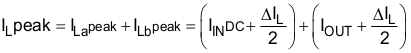
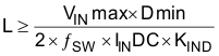
With an estimated 85% efficiency, the input current is calculated with Equation 9 to be 2.35 A. With KIND of 0.3 and the maximum 18-V input, the minimum inductance is calculated to be 10.5 µH using Equation 41. The nearest standard value of 12 µH is used. As mentioned previously, this equation assumes a coupled inductor is used.
The inductor ripple current is recalculated to be 615 mA with Equation 42. The peak current is calculated to
3.69 A. The typical current limit is used as the saturation rating for the inductor used. The RMS current for La is approximately the average input current 2.35 A. The RMS current for Lb is approximately the output current of
1 A. For this design, a CoilCraft MSD1260-123 is used with 6.86-A saturation, 74-mΩ DCR, and 3.12-A RMS current rating for one winding.