SLVSCG7A July 2014 – September 2021 TPS55340-EP
PRODUCTION DATA
- 1 Features
- 2 Applications
- 3 Description
- 4 Revision History
- 5 Description (continued)
- 6 Pin Configuration and Functions
- 7 Specifications
-
8 Detailed Description
- 8.1 Overview
- 8.2 Functional Block Diagram
- 8.3
Feature Description
- 8.3.1 Switching Frequency
- 8.3.2 Voltage Reference and Setting Output Voltage
- 8.3.3 Soft Start
- 8.3.4 Slope Compensation
- 8.3.5 Overcurrent Protection and Frequency Foldback
- 8.3.6 Enable and Thermal Shutdown
- 8.3.7 Undervoltage Lockout (UVLO)
- 8.3.8 Minimum On-Time and Pulse Skipping
- 8.3.9 Layout Considerations
- 8.3.10 Thermal Considerations
- 8.4 Device Functional Modes
-
9 Application and Implementation
- 9.1 Application Information
- 9.2
Typical Applications
- 9.2.1
Boost Converter Application
- 9.2.1.1 Design Requirements
- 9.2.1.2
Detailed Design Procedure
- 9.2.1.2.1 Selecting the Switching Frequency (R4)
- 9.2.1.2.2 Determining the Duty Cycle
- 9.2.1.2.3 Selecting the Inductor (L1)
- 9.2.1.2.4 Computing the Maximum Output Current
- 9.2.1.2.5 Selecting the Output Capacitor (C8 to C10)
- 9.2.1.2.6 Selecting the Input Capacitors (C2, C7)
- 9.2.1.2.7 Setting Output Voltage (R1, R2)
- 9.2.1.2.8 Setting the Soft-Start Time (C7)
- 9.2.1.2.9 Selecting the Schottky Diode (D1)
- 9.2.1.2.10 Compensating the Control Loop (R3, C4, C5)
- 9.2.1.3 Application Curves
- 9.2.2
SEPIC Converter Application
- 9.2.2.1 Design Requirements
- 9.2.2.2
Detailed Design Procedure
- 9.2.2.2.1 Selecting the Switching Frequency (R4)
- 9.2.2.2.2 Duty Cycle
- 9.2.2.2.3 Selecting the Inductor (L1)
- 9.2.2.2.4 Calculating the Maximum Output Current
- 9.2.2.2.5 Selecting the Output Capacitor (C8 to C10)
- 9.2.2.2.6 Selecting the Series Capacitor (C6)
- 9.2.2.2.7 Selecting the Input Capacitor (C2, C7)
- 9.2.2.2.8 Selecting the Schottky Diode (D1)
- 9.2.2.2.9 Setting the Output Voltage (R1, R2)
- 9.2.2.2.10 Setting the Soft-Start Time (C3)
- 9.2.2.2.11 MOSFET Rating Considerations
- 9.2.2.2.12 Compensating the Control Loop (R3, C4)
- 9.2.2.3 SEPIC Converter Application Curves
- 9.2.1
Boost Converter Application
- 10Power Supply Recommendations
- 11Layout
- 12Device and Documentation Support
- 13Mechanical, Packaging, and Orderable Information
Package Options
Mechanical Data (Package|Pins)
- RTE|16
Thermal pad, mechanical data (Package|Pins)
- RTE|16
Orderable Information
9.2.1.2.6 Selecting the Input Capacitors (C2, C7)
TI recommends at least 4.7 µF of ceramic input capacitance. Additional input capacitance may be required to meet ripple and transient requirements. TI recommends a high-quality ceramic, type X5R or X7R to minimize capacitance variations over temperature. The capacitor must also have an RMS current rating greater than the maximum RMS input current of the TPS55340-EP calculated with Equation 22. The input capacitor must also be rated greater than the maximum input voltage. The input voltage ripple can be calculated with Equation 23.
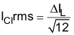
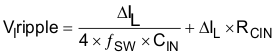
In the design example, the input RMS current is calculated to be 191 mA. The chosen input capacitor is a 10-µF, 35-V 1210 X7R with 3-mΩ ESR. Although one with a lower voltage rating can be used, a 35-V rated capacitor was chosen to limit the affects of DC bias and to allow the circuit to be rated for the entire input range of the TPS55340-EP. The input ripple is calculated to be 30 mV. An additional 0.1-µF, 50-V 0603 X5R is located close to the VIN and GND pins for extra decoupling.