SLVSCG7A July 2014 – September 2021 TPS55340-EP
PRODUCTION DATA
- 1 Features
- 2 Applications
- 3 Description
- 4 Revision History
- 5 Description (continued)
- 6 Pin Configuration and Functions
- 7 Specifications
-
8 Detailed Description
- 8.1 Overview
- 8.2 Functional Block Diagram
- 8.3
Feature Description
- 8.3.1 Switching Frequency
- 8.3.2 Voltage Reference and Setting Output Voltage
- 8.3.3 Soft Start
- 8.3.4 Slope Compensation
- 8.3.5 Overcurrent Protection and Frequency Foldback
- 8.3.6 Enable and Thermal Shutdown
- 8.3.7 Undervoltage Lockout (UVLO)
- 8.3.8 Minimum On-Time and Pulse Skipping
- 8.3.9 Layout Considerations
- 8.3.10 Thermal Considerations
- 8.4 Device Functional Modes
-
9 Application and Implementation
- 9.1 Application Information
- 9.2
Typical Applications
- 9.2.1
Boost Converter Application
- 9.2.1.1 Design Requirements
- 9.2.1.2
Detailed Design Procedure
- 9.2.1.2.1 Selecting the Switching Frequency (R4)
- 9.2.1.2.2 Determining the Duty Cycle
- 9.2.1.2.3 Selecting the Inductor (L1)
- 9.2.1.2.4 Computing the Maximum Output Current
- 9.2.1.2.5 Selecting the Output Capacitor (C8 to C10)
- 9.2.1.2.6 Selecting the Input Capacitors (C2, C7)
- 9.2.1.2.7 Setting Output Voltage (R1, R2)
- 9.2.1.2.8 Setting the Soft-Start Time (C7)
- 9.2.1.2.9 Selecting the Schottky Diode (D1)
- 9.2.1.2.10 Compensating the Control Loop (R3, C4, C5)
- 9.2.1.3 Application Curves
- 9.2.2
SEPIC Converter Application
- 9.2.2.1 Design Requirements
- 9.2.2.2
Detailed Design Procedure
- 9.2.2.2.1 Selecting the Switching Frequency (R4)
- 9.2.2.2.2 Duty Cycle
- 9.2.2.2.3 Selecting the Inductor (L1)
- 9.2.2.2.4 Calculating the Maximum Output Current
- 9.2.2.2.5 Selecting the Output Capacitor (C8 to C10)
- 9.2.2.2.6 Selecting the Series Capacitor (C6)
- 9.2.2.2.7 Selecting the Input Capacitor (C2, C7)
- 9.2.2.2.8 Selecting the Schottky Diode (D1)
- 9.2.2.2.9 Setting the Output Voltage (R1, R2)
- 9.2.2.2.10 Setting the Soft-Start Time (C3)
- 9.2.2.2.11 MOSFET Rating Considerations
- 9.2.2.2.12 Compensating the Control Loop (R3, C4)
- 9.2.2.3 SEPIC Converter Application Curves
- 9.2.1
Boost Converter Application
- 10Power Supply Recommendations
- 11Layout
- 12Device and Documentation Support
- 13Mechanical, Packaging, and Orderable Information
Package Options
Mechanical Data (Package|Pins)
- RTE|16
Thermal pad, mechanical data (Package|Pins)
- RTE|16
Orderable Information
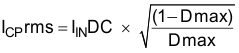
9.2.2.2.6 Selecting the Series Capacitor (C6)
The series capacitor is chosen to limit the ripple current to 5% of the maximum input voltage. Using Equation 47, the minimum capacitance is 1.5 µF. Using Equation 48, the RMS current is calculated to be 1.63 A. A 2.2-µF ceramic capacitor in a 1206 package is selected.
Equation 47. 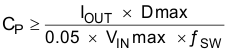
Equation 48.