SLVSCG7A July 2014 – September 2021 TPS55340-EP
PRODUCTION DATA
- 1 Features
- 2 Applications
- 3 Description
- 4 Revision History
- 5 Description (continued)
- 6 Pin Configuration and Functions
- 7 Specifications
-
8 Detailed Description
- 8.1 Overview
- 8.2 Functional Block Diagram
- 8.3
Feature Description
- 8.3.1 Switching Frequency
- 8.3.2 Voltage Reference and Setting Output Voltage
- 8.3.3 Soft Start
- 8.3.4 Slope Compensation
- 8.3.5 Overcurrent Protection and Frequency Foldback
- 8.3.6 Enable and Thermal Shutdown
- 8.3.7 Undervoltage Lockout (UVLO)
- 8.3.8 Minimum On-Time and Pulse Skipping
- 8.3.9 Layout Considerations
- 8.3.10 Thermal Considerations
- 8.4 Device Functional Modes
-
9 Application and Implementation
- 9.1 Application Information
- 9.2
Typical Applications
- 9.2.1
Boost Converter Application
- 9.2.1.1 Design Requirements
- 9.2.1.2
Detailed Design Procedure
- 9.2.1.2.1 Selecting the Switching Frequency (R4)
- 9.2.1.2.2 Determining the Duty Cycle
- 9.2.1.2.3 Selecting the Inductor (L1)
- 9.2.1.2.4 Computing the Maximum Output Current
- 9.2.1.2.5 Selecting the Output Capacitor (C8 to C10)
- 9.2.1.2.6 Selecting the Input Capacitors (C2, C7)
- 9.2.1.2.7 Setting Output Voltage (R1, R2)
- 9.2.1.2.8 Setting the Soft-Start Time (C7)
- 9.2.1.2.9 Selecting the Schottky Diode (D1)
- 9.2.1.2.10 Compensating the Control Loop (R3, C4, C5)
- 9.2.1.3 Application Curves
- 9.2.2
SEPIC Converter Application
- 9.2.2.1 Design Requirements
- 9.2.2.2
Detailed Design Procedure
- 9.2.2.2.1 Selecting the Switching Frequency (R4)
- 9.2.2.2.2 Duty Cycle
- 9.2.2.2.3 Selecting the Inductor (L1)
- 9.2.2.2.4 Calculating the Maximum Output Current
- 9.2.2.2.5 Selecting the Output Capacitor (C8 to C10)
- 9.2.2.2.6 Selecting the Series Capacitor (C6)
- 9.2.2.2.7 Selecting the Input Capacitor (C2, C7)
- 9.2.2.2.8 Selecting the Schottky Diode (D1)
- 9.2.2.2.9 Setting the Output Voltage (R1, R2)
- 9.2.2.2.10 Setting the Soft-Start Time (C3)
- 9.2.2.2.11 MOSFET Rating Considerations
- 9.2.2.2.12 Compensating the Control Loop (R3, C4)
- 9.2.2.3 SEPIC Converter Application Curves
- 9.2.1
Boost Converter Application
- 10Power Supply Recommendations
- 11Layout
- 12Device and Documentation Support
- 13Mechanical, Packaging, and Orderable Information
Package Options
Mechanical Data (Package|Pins)
- RTE|16
Thermal pad, mechanical data (Package|Pins)
- RTE|16
Orderable Information
8.3.4 Slope Compensation
The TPS55340-EP has internal slope compensation to prevent subharmonic oscillations. The sensed current slope of boost converter can be expressed as Equation 4.
Equation 4. 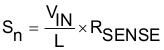
Calculate the slope compensation dv/dt using Equation 5.
Equation 5. 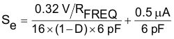
In a converter with current mode control, in addition to the output voltage feedback loop, take into account the inner current loop including the inductor current sampling effect and slope compensation on the small signal response, which can be modeled as seen in Equation 6.
Equation 6. 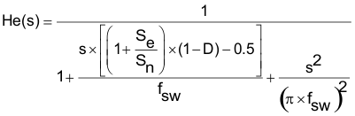
where
- RSENSE (15 mΩ) is the equivalent current sense resistor
- RFREQ is timing resistor used to set frequency
- D is the duty cycle
Note that if Sn << Se, the converter operates in voltage mode control rather than current mode control, and Equation 6 is no longer valid.