SLVSCG7A July 2014 – September 2021 TPS55340-EP
PRODUCTION DATA
- 1 Features
- 2 Applications
- 3 Description
- 4 Revision History
- 5 Description (continued)
- 6 Pin Configuration and Functions
- 7 Specifications
-
8 Detailed Description
- 8.1 Overview
- 8.2 Functional Block Diagram
- 8.3
Feature Description
- 8.3.1 Switching Frequency
- 8.3.2 Voltage Reference and Setting Output Voltage
- 8.3.3 Soft Start
- 8.3.4 Slope Compensation
- 8.3.5 Overcurrent Protection and Frequency Foldback
- 8.3.6 Enable and Thermal Shutdown
- 8.3.7 Undervoltage Lockout (UVLO)
- 8.3.8 Minimum On-Time and Pulse Skipping
- 8.3.9 Layout Considerations
- 8.3.10 Thermal Considerations
- 8.4 Device Functional Modes
-
9 Application and Implementation
- 9.1 Application Information
- 9.2
Typical Applications
- 9.2.1
Boost Converter Application
- 9.2.1.1 Design Requirements
- 9.2.1.2
Detailed Design Procedure
- 9.2.1.2.1 Selecting the Switching Frequency (R4)
- 9.2.1.2.2 Determining the Duty Cycle
- 9.2.1.2.3 Selecting the Inductor (L1)
- 9.2.1.2.4 Computing the Maximum Output Current
- 9.2.1.2.5 Selecting the Output Capacitor (C8 to C10)
- 9.2.1.2.6 Selecting the Input Capacitors (C2, C7)
- 9.2.1.2.7 Setting Output Voltage (R1, R2)
- 9.2.1.2.8 Setting the Soft-Start Time (C7)
- 9.2.1.2.9 Selecting the Schottky Diode (D1)
- 9.2.1.2.10 Compensating the Control Loop (R3, C4, C5)
- 9.2.1.3 Application Curves
- 9.2.2
SEPIC Converter Application
- 9.2.2.1 Design Requirements
- 9.2.2.2
Detailed Design Procedure
- 9.2.2.2.1 Selecting the Switching Frequency (R4)
- 9.2.2.2.2 Duty Cycle
- 9.2.2.2.3 Selecting the Inductor (L1)
- 9.2.2.2.4 Calculating the Maximum Output Current
- 9.2.2.2.5 Selecting the Output Capacitor (C8 to C10)
- 9.2.2.2.6 Selecting the Series Capacitor (C6)
- 9.2.2.2.7 Selecting the Input Capacitor (C2, C7)
- 9.2.2.2.8 Selecting the Schottky Diode (D1)
- 9.2.2.2.9 Setting the Output Voltage (R1, R2)
- 9.2.2.2.10 Setting the Soft-Start Time (C3)
- 9.2.2.2.11 MOSFET Rating Considerations
- 9.2.2.2.12 Compensating the Control Loop (R3, C4)
- 9.2.2.3 SEPIC Converter Application Curves
- 9.2.1
Boost Converter Application
- 10Power Supply Recommendations
- 11Layout
- 12Device and Documentation Support
- 13Mechanical, Packaging, and Orderable Information
Package Options
Mechanical Data (Package|Pins)
- RTE|16
Thermal pad, mechanical data (Package|Pins)
- RTE|16
Orderable Information
9.2.1.2.7 Setting Output Voltage (R1, R2)
To set the output voltage in either DCM or CCM, select the values of R1 and R2 according to Equation 24 and Equation 25.
Equation 24. 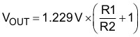
Equation 25. 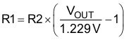
Considering the leakage current through the resistor divider and noise decoupling into FB pin, an optimum value for R2 is around 10 kΩ. The output voltage tolerance depends on the VFB accuracy and the tolerance of R1 and R2. In this example with a 24-V output using Equation 25, R1 is calculated to 185.3 kΩ. The nearest standard value of 187 kΩ is used.