SLVSD05H March 2016 – June 2025 TPS56C215
PRODUCTION DATA
- 1
- 1 Features
- 2 Applications
- 3 Description
- 4 Pin Configuration and Functions
- 5 Specifications
-
6 Detailed Description
- 6.1 Overview
- 6.2 Functional Block Diagram
- 6.3
Feature Description
- 6.3.1 PWM Operation and D-CAP3™ Control Mode
- 6.3.2 Eco-mode Control
- 6.3.3 4.7-V LDO
- 6.3.4 MODE Selection
- 6.3.5 Soft Start and Prebiased Soft Start
- 6.3.6 Enable and Adjustable UVLO
- 6.3.7 Power Good
- 6.3.8 Overcurrent Protection and Undervoltage Protection
- 6.3.9 Transient Response Enhancement
- 6.3.10 UVLO Protection
- 6.3.11 Thermal Shutdown
- 6.3.12 Output Voltage Discharge
- 6.4 Device Functional Modes
- 7 Application and Implementation
- 8 Device and Documentation Support
- 9 Revision History
- 10Mechanical, Packaging, and Orderable Information
Package Options
Mechanical Data (Package|Pins)
- RNN|18
Thermal pad, mechanical data (Package|Pins)
Orderable Information
7.2.2.2.3 Inductor Selection
The inductor ripple current is filtered by the output capacitor. A higher inductor ripple current means the output capacitor must have a ripple current rating higher than the inductor ripple current. See Table 7-2 for recommended inductor values.
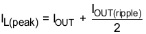
The RMS and peak currents through the inductor can be calculated using Equation 7 and Equation 8. MAke sure that the inductor is rated to handle these currents.

During transient, short circuit conditions, the inductor current can increase up to the current limit of the device so choosing an inductor with a saturation current higher than the peak current under current limit condition is safe.