SLVSD05H March 2016 – June 2025 TPS56C215
PRODUCTION DATA
- 1
- 1 Features
- 2 Applications
- 3 Description
- 4 Pin Configuration and Functions
- 5 Specifications
-
6 Detailed Description
- 6.1 Overview
- 6.2 Functional Block Diagram
- 6.3
Feature Description
- 6.3.1 PWM Operation and D-CAP3™ Control Mode
- 6.3.2 Eco-mode Control
- 6.3.3 4.7-V LDO
- 6.3.4 MODE Selection
- 6.3.5 Soft Start and Prebiased Soft Start
- 6.3.6 Enable and Adjustable UVLO
- 6.3.7 Power Good
- 6.3.8 Overcurrent Protection and Undervoltage Protection
- 6.3.9 Transient Response Enhancement
- 6.3.10 UVLO Protection
- 6.3.11 Thermal Shutdown
- 6.3.12 Output Voltage Discharge
- 6.4 Device Functional Modes
- 7 Application and Implementation
- 8 Device and Documentation Support
- 9 Revision History
- 10Mechanical, Packaging, and Orderable Information
Package Options
Mechanical Data (Package|Pins)
- RNN|18
Thermal pad, mechanical data (Package|Pins)
Orderable Information
6.3.2 Eco-mode Control
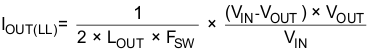
The TPS56C215 is designed with Eco-mode control to increase efficiency at light loads. This option can be chosen using the MODE pin as shown in Table 6-3. As the output current decreases from heavy load condition, the inductor current is also reduced. If the output current is reduced enough, the valley of the inductor current reaches the zero level, which is the boundary between continuous conduction and discontinuous conduction modes. The low-side MOSFET is turned off when a zero inductor current is detected. As the load current further decreases the converter runs into discontinuous conduction mode. The on-time is kept approximately the same as in continuous conduction mode. The off-time increases as discharging the output with a smaller load current takes more time. The light load current where the transition to Eco-mode operation happens (IOUT(LL)) can be calculated from Equation 2.
After identifying the application requirements, design the output inductance (LOUT) so that the inductor peak-to-peak ripple current is approximately between 20% and 30% of the IOUT(ma×) (peak current in the application). Sizing the inductor properly so that the valley current does not hit the negative low-side current limit is important.