SLVSDQ7B October 2016 – July 2021 TPS57114C-Q1
PRODUCTION DATA
- 1 Features
- 2 Applications
- 3 Description
- 4 Revision History
- 5 Pin Configuration and Functions
- 6 Specifications
-
7 Detailed Description
- 7.1 Overview
- 7.2 Functional Block Diagram
- 7.3 Feature Description
- 7.4
Device Functional Modes
- 7.4.1 Adjusting the Output Voltage
- 7.4.2 Enable Functionality and Adjusting Undervoltage Lockout
- 7.4.3 Slow-Start or Tracking Pin
- 7.4.4 Sequencing
- 7.4.5 Constant Switching Frequency and Timing Resistor (RT/CLK Pin)
- 7.4.6 Overcurrent Protection
- 7.4.7 Frequency Shift
- 7.4.8 Reverse Overcurrent Protection
- 7.4.9 Synchronize Using The RT/CLK Pin
- 7.4.10 Power Good (PWRGD Pin)
- 7.4.11 Overvoltage Transient Protection
- 7.4.12 Thermal Shutdown
- 7.4.13 Small-Signal Model for Loop Response
- 7.4.14 Simple Small-Signal Model for Peak-Current Mode Control
- 7.4.15 Small-Signal Model for Frequency Compensation
-
8 Application and Implementation
- 8.1 Application Information
- 8.2
Typical Application
- 8.2.1 Design Requirements
- 8.2.2
Detailed Design Procedure
- 8.2.2.1 Selecting the Switching Frequency
- 8.2.2.2 Output Inductor Selection
- 8.2.2.3 Output Capacitor
- 8.2.2.4 Input Capacitor
- 8.2.2.5 Slow-Start Capacitor
- 8.2.2.6 Bootstrap Capacitor Selection
- 8.2.2.7 Output-Voltage And Feedback-Resistor Selection
- 8.2.2.8 Compensation
- 8.2.2.9 Power-Dissipation Estimate
- 8.2.3 Application Curves
- 9 Power Supply Recommendations
- 10Layout
- 11Device and Documentation Support
- 12Mechanical, Packaging, and Orderable Information
Package Options
Mechanical Data (Package|Pins)
- RTE|16
Thermal pad, mechanical data (Package|Pins)
- RTE|16
Orderable Information
8.2.2.3 Output Capacitor
There are three primary considerations for selecting the value of the output capacitor. The output capacitor determines the modulator pole, the output-voltage ripple, and how the regulator responds to a large change in load current. Base the output-capacitance selection on the most stringent of these three criteria.
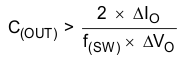
The desired response to a large change in the load current is the first criterion. The output capacitor must supply the load with current when the regulator cannot. This situation would occur if there are desired hold-up times for the regulator where the output capacitor must hold the output voltage above a certain level for a specified amount of time after removal of the input power. The regulator is temporarily not able to supply sufficient output current if there is a large, fast increase in the current requirement of the load, such as transitioning from no load to a full load. The regulator usually requires two or more clock cycles for the control loop to see the change in load current and output voltage and then adjust the duty cycle to react to the change. The output capacitor must be large enough to supply the extra current to the load until the control loop responds to the load change. The output capacitance must be large enough to supply the difference in current for two clock cycles while only allowing a tolerable amount of droop in the output voltage. Equation 26 shows the minimum output capacitance necessary to meet this requirement.
For this example, the transient load response is specified as a 5% change in VO for a load step from 0 A (no load) to 1.5 A. For this example, ΔI(out) = 1.5 – 0 = 1.5 A and ΔV(out) = 0.05 × 1.8 = 0.09 V. Using these numbers gives a minimum capacitance of 33 µF. This value does not take the ESR of the output capacitor into account in the output voltage change. For ceramic capacitors, the ESR is usually small enough to ignore in this calculation.
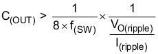
Equation 27 calculates the minimum output capacitance needed to meet the output-voltage ripple specification. In this case, the maximum output voltage ripple is 30 mV. Under this requirement, Equation 27 yields 2.3 µF.
where
- ΔIO is the change in output current
- f(SW) is the regulator switching frequency
- ΔVO is the allowable change in the output voltage
where
- f(SW) is the switching frequency
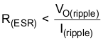
- VO(ripple) is the maximum allowable output voltage ripple
- I(ripple) is the inductor ripple current.
Equation 28 calculates the maximum ESR an output capacitor can have to meet the output-voltage ripple specification. Equation 28 indicates the ESR should be less than 55 mΩ. In this case, the ESR of the ceramic capacitor is much less than 55 mΩ.
Factoring in additional capacitance deratings for aging, temperature, and dc bias increases this minimum value. This example uses two 22-µF, 10-V X5R ceramic capacitors with 3 mΩ of ESR.
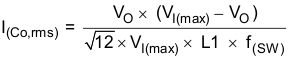
Capacitors generally have limits to the amount of ripple current they can handle without failing or producing excess heat. Select an output capacitor that can support the inductor ripple current. Some capacitor data sheets specify the root-mean-square (rms) value of the maximum ripple current. Use Equation 29 to calculate the rms ripple current that the output capacitor must support. For this application, Equation 29 yields 333 mA.