SLVSDQ7B October 2016 – July 2021 TPS57114C-Q1
PRODUCTION DATA
- 1 Features
- 2 Applications
- 3 Description
- 4 Revision History
- 5 Pin Configuration and Functions
- 6 Specifications
-
7 Detailed Description
- 7.1 Overview
- 7.2 Functional Block Diagram
- 7.3 Feature Description
- 7.4
Device Functional Modes
- 7.4.1 Adjusting the Output Voltage
- 7.4.2 Enable Functionality and Adjusting Undervoltage Lockout
- 7.4.3 Slow-Start or Tracking Pin
- 7.4.4 Sequencing
- 7.4.5 Constant Switching Frequency and Timing Resistor (RT/CLK Pin)
- 7.4.6 Overcurrent Protection
- 7.4.7 Frequency Shift
- 7.4.8 Reverse Overcurrent Protection
- 7.4.9 Synchronize Using The RT/CLK Pin
- 7.4.10 Power Good (PWRGD Pin)
- 7.4.11 Overvoltage Transient Protection
- 7.4.12 Thermal Shutdown
- 7.4.13 Small-Signal Model for Loop Response
- 7.4.14 Simple Small-Signal Model for Peak-Current Mode Control
- 7.4.15 Small-Signal Model for Frequency Compensation
-
8 Application and Implementation
- 8.1 Application Information
- 8.2
Typical Application
- 8.2.1 Design Requirements
- 8.2.2
Detailed Design Procedure
- 8.2.2.1 Selecting the Switching Frequency
- 8.2.2.2 Output Inductor Selection
- 8.2.2.3 Output Capacitor
- 8.2.2.4 Input Capacitor
- 8.2.2.5 Slow-Start Capacitor
- 8.2.2.6 Bootstrap Capacitor Selection
- 8.2.2.7 Output-Voltage And Feedback-Resistor Selection
- 8.2.2.8 Compensation
- 8.2.2.9 Power-Dissipation Estimate
- 8.2.3 Application Curves
- 9 Power Supply Recommendations
- 10Layout
- 11Device and Documentation Support
- 12Mechanical, Packaging, and Orderable Information
Package Options
Mechanical Data (Package|Pins)
- RTE|16
Thermal pad, mechanical data (Package|Pins)
- RTE|16
Orderable Information
8.2.2.8 Compensation
There are several industry techniques used to compensate dc-dc regulators. The method presented here is easy to calculate and yields high phase margins. For most conditions, the regulator has a phase margin between 60 and 90 degrees. The method presented here ignores the effects of the slope compensation that is internal to the TPS57114C-Q1 device. Because of ignoring the slope compensation, the actual crossover frequency is usually lower than the crossover frequency used in the calculations. Use SwitcherPro software for a more-accurate design.
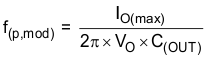
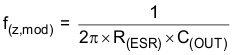
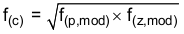
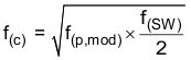
To get started, calculate the modulator pole, f(p,mod), and the ESR zero, f(z, mod), using Equation 36 and Equation 37. For C(OUT), derating the capacitor is not necessary, as the 1.8-V output is a small percentage of the 10-V capacitor rating. If the output is a high percentage of the capacitor rating, use the manufacturer information for the capacitor to derate the capacitor value. Use Equation 38 and Equation 39 to estimate a starting point for the crossover frequency, f(c). For the example design, f(p,mod) is 6.03 kHz and f(z,mod) is 1210 kHz. Equation 38 is the geometric mean of the modulator pole and the ESR zero and Equation 39 is the mean of the modulator pole and the switching frequency. Equation 38 yields 85.3 kHz and Equation 39 gives 54.9 kHz. Use the lower value of Equation 38 or Equation 39 as the approximate crossover frequency. For this example, f(c) is 56 kHz. Next, calculate the compensation components. Use a resistor in series with a capacitor to create a compensating zero. A capacitor in parallel with these two components forms the compensating pole (if needed).
The compensation design takes the following steps:
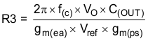
- Set up the anticipated crossover frequency. Use Equation 40 to calculate the resistor value for the compensation network. In this example, the anticipated crossover frequency (f(c)) is 56 kHz. The power-stage gain (gm(ps)) is 25 S, and the error-amplifier gain (gm(ea)) is 245 µS.
Equation 40.
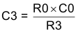
- Place compensation zero at the pole formed by the load resistor and the output capacitor. Calculate the capacitor for the compensation network using Equation 41.
Equation 41.
- One can include an additional pole to attenuate high-frequency noise. In this application, the extra pole is not necessary.
From the preceding procedures, the compensation network includes a 7.68-kΩ resistor and a 3300-pF capacitor.