SLVSDQ7B October 2016 – July 2021 TPS57114C-Q1
PRODUCTION DATA
- 1 Features
- 2 Applications
- 3 Description
- 4 Revision History
- 5 Pin Configuration and Functions
- 6 Specifications
-
7 Detailed Description
- 7.1 Overview
- 7.2 Functional Block Diagram
- 7.3 Feature Description
- 7.4
Device Functional Modes
- 7.4.1 Adjusting the Output Voltage
- 7.4.2 Enable Functionality and Adjusting Undervoltage Lockout
- 7.4.3 Slow-Start or Tracking Pin
- 7.4.4 Sequencing
- 7.4.5 Constant Switching Frequency and Timing Resistor (RT/CLK Pin)
- 7.4.6 Overcurrent Protection
- 7.4.7 Frequency Shift
- 7.4.8 Reverse Overcurrent Protection
- 7.4.9 Synchronize Using The RT/CLK Pin
- 7.4.10 Power Good (PWRGD Pin)
- 7.4.11 Overvoltage Transient Protection
- 7.4.12 Thermal Shutdown
- 7.4.13 Small-Signal Model for Loop Response
- 7.4.14 Simple Small-Signal Model for Peak-Current Mode Control
- 7.4.15 Small-Signal Model for Frequency Compensation
-
8 Application and Implementation
- 8.1 Application Information
- 8.2
Typical Application
- 8.2.1 Design Requirements
- 8.2.2
Detailed Design Procedure
- 8.2.2.1 Selecting the Switching Frequency
- 8.2.2.2 Output Inductor Selection
- 8.2.2.3 Output Capacitor
- 8.2.2.4 Input Capacitor
- 8.2.2.5 Slow-Start Capacitor
- 8.2.2.6 Bootstrap Capacitor Selection
- 8.2.2.7 Output-Voltage And Feedback-Resistor Selection
- 8.2.2.8 Compensation
- 8.2.2.9 Power-Dissipation Estimate
- 8.2.3 Application Curves
- 9 Power Supply Recommendations
- 10Layout
- 11Device and Documentation Support
- 12Mechanical, Packaging, and Orderable Information
Package Options
Mechanical Data (Package|Pins)
- RTE|16
Thermal pad, mechanical data (Package|Pins)
- RTE|16
Orderable Information
7.4.2 Enable Functionality and Adjusting Undervoltage Lockout
The VIN pin voltage falling below 2.6 V disables the TPS57114C-Q1 device. If an application requires a higher undervoltage lockout (UVLO), use the EN pin as shown in Figure 7-2 to adjust the input voltage UVLO by connecting two external resistors. TI recommends using the EN resistors to set the UVLO falling threshold (V(STOP)) above 2.6 V. Set the rising threshold (V(START)) to provide enough hysteresis to allow for any input supply variations. The EN pin has an internal pullup current source that provides the default condition of the TPS57114C-Q1 operation when the EN pin floats. Once the EN pin voltage exceeds 1.25 V, the circuitry adds an additional 1.6 µA of hysteresis. Pulling the EN pin below 1.18 V removes the 1.6 µA. This additional current facilitates input voltage hysteresis.
 Figure 7-2 Adjustable Undervoltage Lockout
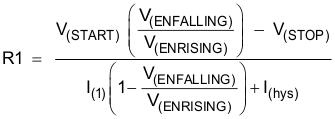
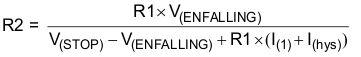
where I(hys) = 1.6 µA, I(1) = 1.6 µA, V(ENRISING) = 1.25 V, V(ENFALLING) = 1.18 V.