SLVSDQ7B October 2016 – July 2021 TPS57114C-Q1
PRODUCTION DATA
- 1 Features
- 2 Applications
- 3 Description
- 4 Revision History
- 5 Pin Configuration and Functions
- 6 Specifications
-
7 Detailed Description
- 7.1 Overview
- 7.2 Functional Block Diagram
- 7.3 Feature Description
- 7.4
Device Functional Modes
- 7.4.1 Adjusting the Output Voltage
- 7.4.2 Enable Functionality and Adjusting Undervoltage Lockout
- 7.4.3 Slow-Start or Tracking Pin
- 7.4.4 Sequencing
- 7.4.5 Constant Switching Frequency and Timing Resistor (RT/CLK Pin)
- 7.4.6 Overcurrent Protection
- 7.4.7 Frequency Shift
- 7.4.8 Reverse Overcurrent Protection
- 7.4.9 Synchronize Using The RT/CLK Pin
- 7.4.10 Power Good (PWRGD Pin)
- 7.4.11 Overvoltage Transient Protection
- 7.4.12 Thermal Shutdown
- 7.4.13 Small-Signal Model for Loop Response
- 7.4.14 Simple Small-Signal Model for Peak-Current Mode Control
- 7.4.15 Small-Signal Model for Frequency Compensation
-
8 Application and Implementation
- 8.1 Application Information
- 8.2
Typical Application
- 8.2.1 Design Requirements
- 8.2.2
Detailed Design Procedure
- 8.2.2.1 Selecting the Switching Frequency
- 8.2.2.2 Output Inductor Selection
- 8.2.2.3 Output Capacitor
- 8.2.2.4 Input Capacitor
- 8.2.2.5 Slow-Start Capacitor
- 8.2.2.6 Bootstrap Capacitor Selection
- 8.2.2.7 Output-Voltage And Feedback-Resistor Selection
- 8.2.2.8 Compensation
- 8.2.2.9 Power-Dissipation Estimate
- 8.2.3 Application Curves
- 9 Power Supply Recommendations
- 10Layout
- 11Device and Documentation Support
- 12Mechanical, Packaging, and Orderable Information
Package Options
Mechanical Data (Package|Pins)
- RTE|16
Thermal pad, mechanical data (Package|Pins)
- RTE|16
Orderable Information
3 Description
The TPS57114C-Q1 device is a full-featured 6-V, 4-A, synchronous step-down current-mode converter with two integrated MOSFETs.
The TPS57114C-Q1 device enables small designs by integrating the MOSFETs, implementing current-mode control to reduce external component count, reducing inductor size by enabling up to 2-MHz switching frequency, and minimizing the IC footprint with a small 3-mm × 3-mm thermally enhanced QFN package.
The TPS57114C-Q1 device provides accurate regulation for a variety of loads with an accurate ±1% voltage reference (Vref) over temperature.
Efficiency is maximized through the integrated 12-mΩ MOSFETs and 515-μA typical supply current. Using the enable pin, shutdown supply current is reduced to 5.5 µA by entering a shutdown mode.
The internal undervoltage lockout setting is 2.45 V, but programming the threshold with a resistor network on the enable pin can increase the setting. The slow-start pin controls the output-voltage start-up ramp. An open-drain power-good signal indicates the output is within 93% to 107% of the nominal voltage.
Frequency foldback and thermal shutdown protect the device during an overcurrent condition.
| PART NUMBER | PACKAGE(1) | BODY SIZE (NOM) |
|---|---|---|
| TPS57114C-Q1 | WQFN (16) | 3.00 mm × 3.00 mm |
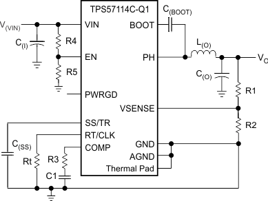
 Simplified Schematic
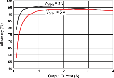
 Efficiency Curve