SLVSCQ9E November 2014 – March 2022 TPS65400
PRODUCTION DATA
- 1 Features
- 2 Applications
- 3 Description
- 4 Revision History
- 5 Description (continued)
- 6 Pin Configuration and Functions
- 7 Specifications
-
8 Detailed Description
- 8.1 Overview
- 8.2 Functional Block Diagrams
- 8.3
Feature Description
- 8.3.1 Startup Timing and Power Sequencing
- 8.3.2 UVLO and Precision Enables
- 8.3.3 Soft-Start and Prebiased Startup
- 8.3.4 PWM Switching Frequency Selection
- 8.3.5 Clock Synchronization
- 8.3.6 Phase Interleaving
- 8.3.7 Fault Handling
- 8.3.8 OCP for SW1 to SW4
- 8.3.9 Overcurrent Protection for SW1 to SW4 in Current Sharing Operation
- 8.3.10 Recovery on Power Loss
- 8.3.11 Feedback Compensation
- 8.3.12 Adjusting Output Voltage
- 8.3.13 Digital Interface – PMBus
- 8.3.14 Initial Configuration
- 8.4 Device Functional Modes
- 8.5 Programming
- 8.6
Register Maps
- 8.6.1
PMBus Core Commands
- 8.6.1.1 (00h) PAGE
- 8.6.1.2 (01h) OPERATION
- 8.6.1.3 (03h) CLEAR_FAULTS
- 8.6.1.4 (10h) WRITE_PROTECT
- 8.6.1.5 (11h) STORE_DEFAULT_ALL
- 8.6.1.6 (19h) CAPABILITY
- 8.6.1.7 (78h) STATUS_BYTE
- 8.6.1.8 (79h) STATUS_WORD
- 8.6.1.9 (7Ah) STATUS_VOUT
- 8.6.1.10 (80h) STATUS_MFR_SPECIFIC
- 8.6.1.11 (98h) PMBUS_REVISION
- 8.6.1.12 (ADh) IC_DEVICE_ID
- 8.6.1.13 (AEh) IC_DEVICE_REV
- 8.6.2
Manufacturer-Specific Commands
- 8.6.2.1 (D0h) USER_DATA_BYTE_00
- 8.6.2.2 (D1h) USER_DATA_BYTE_01
- 8.6.2.3 (D2h) PIN_CONFIG_00
- 8.6.2.4 (D3h) PIN_CONFIG_01
- 8.6.2.5 (D4h) SEQUENCE_CONFIG
- 8.6.2.6 (D5h) SEQUENCE_ORDER
- 8.6.2.7 (D6h) IOUT_MODE
- 8.6.2.8 (D7h) FREQUENCY_PHASE
- 8.6.2.9 (D8h) VREF_COMMAND
- 8.6.2.10 (D9h) IOUT_MAX
- 8.6.2.11 (DAh) USER_RAM_00
- 8.6.2.12 (DBh) SOFT_RESET
- 8.6.2.13 (DCh) RESET_DELAY
- 8.6.2.14 (DDh) TON_TOFF_DELAY
- 8.6.2.15 (DEh) TON_TRANSITION_RATE
- 8.6.2.16 (DFh) VREF_TRANSITION_RATE
- 8.6.2.17 (F0h) SLOPE_COMPENSATION
- 8.6.2.18 (F1h) ISENSE_GAIN
- 8.6.2.19 (FCh) DEVICE_CODE
- 8.6.1
PMBus Core Commands
- 9 Application and Implementation
- 10Power Supply Recommendations
- 11Layout
- 12Device and Documentation Support
- 13Mechanical, Packaging, and Orderable Information
Package Options
Mechanical Data (Package|Pins)
- RGZ|48
Thermal pad, mechanical data (Package|Pins)
- RGZ|48
Orderable Information
8.3.5 Clock Synchronization
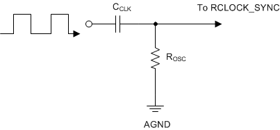
The RCLOCK_SYNC terminal can be used to synchronize the master clock switching frequency, FOSC, with an external clock source or another TPS65400. The external clock signal (which can come from another TPS65400 CLK_OUT terminal) should be AC coupled to the RCLOCK_SYNC terminal as shown in Figure 8-10. Choose the ROSC value so that the fixed frequency is nominally 30% lower than the external synchronizing clock frequency. An internal protection diode clamps the low level of the synchronizing signal to approximately –0.5 V. The internal clock synchronizes to the rising edge of the external clock.
 Figure 8-10 AC-Coupled Clock Synchronization
TI recommends to choose an AC-coupling capacitance in the range of 50 to 100 pF. Exceeding the recommended capacitance may inject excessive energy through the internal clamping diode structure present on the RCLOCK_SYNC terminal. The typical trip level of the synchronization terminal is 1.5 V. To ensure proper synchronization and to avoid damaging the IC, the peak-to-peak value (amplitude) should be between 2.5 V and VDDA. The minimum duration of this pulse must be greater than 200 ns, and its maximum duration must be 200 ns less than the period of the switching cycle.
The external clock synchronization process begins after the TPS65400 is enabled and an external clock signal is detected. The frequency modulator adjusts the oscillator frequency to match the frequency of the pulses into the RCLOCK_SYNC terminal. It generally takes 50 cycles before the PWM frequency locks. If the external clock signal is removed after frequency synchronization, the master clock FOSC drifts to the frequency selected by ROSC.