SLVSCQ9E November 2014 – March 2022 TPS65400
PRODUCTION DATA
- 1 Features
- 2 Applications
- 3 Description
- 4 Revision History
- 5 Description (continued)
- 6 Pin Configuration and Functions
- 7 Specifications
-
8 Detailed Description
- 8.1 Overview
- 8.2 Functional Block Diagrams
- 8.3
Feature Description
- 8.3.1 Startup Timing and Power Sequencing
- 8.3.2 UVLO and Precision Enables
- 8.3.3 Soft-Start and Prebiased Startup
- 8.3.4 PWM Switching Frequency Selection
- 8.3.5 Clock Synchronization
- 8.3.6 Phase Interleaving
- 8.3.7 Fault Handling
- 8.3.8 OCP for SW1 to SW4
- 8.3.9 Overcurrent Protection for SW1 to SW4 in Current Sharing Operation
- 8.3.10 Recovery on Power Loss
- 8.3.11 Feedback Compensation
- 8.3.12 Adjusting Output Voltage
- 8.3.13 Digital Interface – PMBus
- 8.3.14 Initial Configuration
- 8.4 Device Functional Modes
- 8.5 Programming
- 8.6
Register Maps
- 8.6.1
PMBus Core Commands
- 8.6.1.1 (00h) PAGE
- 8.6.1.2 (01h) OPERATION
- 8.6.1.3 (03h) CLEAR_FAULTS
- 8.6.1.4 (10h) WRITE_PROTECT
- 8.6.1.5 (11h) STORE_DEFAULT_ALL
- 8.6.1.6 (19h) CAPABILITY
- 8.6.1.7 (78h) STATUS_BYTE
- 8.6.1.8 (79h) STATUS_WORD
- 8.6.1.9 (7Ah) STATUS_VOUT
- 8.6.1.10 (80h) STATUS_MFR_SPECIFIC
- 8.6.1.11 (98h) PMBUS_REVISION
- 8.6.1.12 (ADh) IC_DEVICE_ID
- 8.6.1.13 (AEh) IC_DEVICE_REV
- 8.6.2
Manufacturer-Specific Commands
- 8.6.2.1 (D0h) USER_DATA_BYTE_00
- 8.6.2.2 (D1h) USER_DATA_BYTE_01
- 8.6.2.3 (D2h) PIN_CONFIG_00
- 8.6.2.4 (D3h) PIN_CONFIG_01
- 8.6.2.5 (D4h) SEQUENCE_CONFIG
- 8.6.2.6 (D5h) SEQUENCE_ORDER
- 8.6.2.7 (D6h) IOUT_MODE
- 8.6.2.8 (D7h) FREQUENCY_PHASE
- 8.6.2.9 (D8h) VREF_COMMAND
- 8.6.2.10 (D9h) IOUT_MAX
- 8.6.2.11 (DAh) USER_RAM_00
- 8.6.2.12 (DBh) SOFT_RESET
- 8.6.2.13 (DCh) RESET_DELAY
- 8.6.2.14 (DDh) TON_TOFF_DELAY
- 8.6.2.15 (DEh) TON_TRANSITION_RATE
- 8.6.2.16 (DFh) VREF_TRANSITION_RATE
- 8.6.2.17 (F0h) SLOPE_COMPENSATION
- 8.6.2.18 (F1h) ISENSE_GAIN
- 8.6.2.19 (FCh) DEVICE_CODE
- 8.6.1
PMBus Core Commands
- 9 Application and Implementation
- 10Power Supply Recommendations
- 11Layout
- 12Device and Documentation Support
- 13Mechanical, Packaging, and Orderable Information
Package Options
Mechanical Data (Package|Pins)
- RGZ|48
Thermal pad, mechanical data (Package|Pins)
- RGZ|48
Orderable Information
8.3.14 Initial Configuration
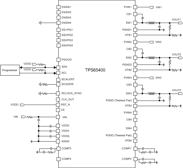
The recommended method of configuring the TPS65400 the first time is through an external programmer through a separate I2C programming header (as shown in Figure 8-15). The programming header needs to connect to the SCL, SDA, CE, VDDD, and DGND lines, and can be done using a USB-to-I2C tool. This enables the user to tailor the settings of the TPS65400 for each PCB specifically after PCB assembly, before the first power-up of the board.
An alternative method is to use the firmware in an on-board microcontroller to do the initial configuration. To do this, the user has two options:
- Power the microcontroller and the TPS65400 (VDDD, CE, and DGND connections needed) from an external source not controlled by the TPS65400.
- Design the PCB so that the default settings of the TPS65400 allow the microcontroller to be powered when power is applied to the TPS65400 the first time. The designer also needs to ensure that the default power-up sequence, ramp-rates, and other default parameters do not damage any components when power is applied the first time. After configuration, the microcontroller should pull CE low, and then all future power-ups result in the newly configured power-up scheme to occur.
Using either method for the microcontroller requires the firmware to check if the TPS65400 has been previously configured, or if a modification needs to be made to an already programmed configuration. Users may use USER_DATA_BYTE_00 and/or USER_DATA_BYTE_01 to store a version number to identify which version of the configuration is stored in the TPS65400.
A hybrid option may also be done where the initial configuration is done using an external programmer, and the subsequent revisions are done through the microcontroller firmware. This eliminates the risk from damage caused by the default configuration during the first power-up, but still allows the microcontroller firmware to modify settings such as the VREF settings for subsequent power-ups.

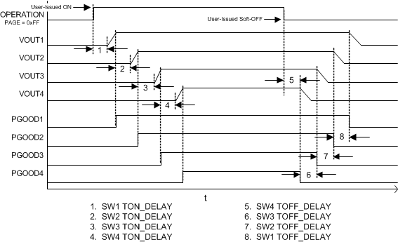
- Enable pins ENSWx set to inactive in PIN_CONFIG_00
- Start sequence order SW1-SW2-SW3-SW4 in SEQUENCE_ORDER
- Stop sequence order SW4-SW3-SW2-SW1 in SEQUENCE_ORDER
OPERATION (SWx) refers to OPERATION register in the corresponding PMBus PAGE. See (01h) OPERATION for more information on the OPERATION register.
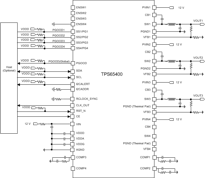
 Figure 8-16 Internal Sequencing Schematic With Host
 Figure 8-17 Internal Sequencing Schematic Without Host