SLVSCQ9E November   2014  – March 2022 TPS65400

PRODUCTION DATA  

  1. Features
  2. Applications
  3. Description
  4. Revision History
  5. Description (continued)
  6. Pin Configuration and Functions
  7. Specifications
    1. 7.1 Absolute Maximum Ratings
    2. 7.2 ESD Ratings
    3. 7.3 Recommended Operating Conditions
    4. 7.4 Thermal Information
    5. 7.5 Electrical Characteristics
    6. 7.6 System Characteristics
    7. 7.7 Operational Parameters
    8. 7.8 Package Dissipation Ratings
    9. 7.9 Typical Characteristics: System Efficiency
  8. Detailed Description
    1. 8.1 Overview
    2. 8.2 Functional Block Diagrams
    3. 8.3 Feature Description
      1. 8.3.1  Startup Timing and Power Sequencing
        1. 8.3.1.1 Startup Timing
        2. 8.3.1.2 External Sequencing
        3. 8.3.1.3 Internal Sequencing
      2. 8.3.2  UVLO and Precision Enables
      3. 8.3.3  Soft-Start and Prebiased Startup
        1. 8.3.3.1 Analog Soft-Start (Default) and Digital Soft-Start
        2. 8.3.3.2 Soft-Start Capacitor Selection
      4. 8.3.4  PWM Switching Frequency Selection
      5. 8.3.5  Clock Synchronization
      6. 8.3.6  Phase Interleaving
      7. 8.3.7  Fault Handling
      8. 8.3.8  OCP for SW1 to SW4
      9. 8.3.9  Overcurrent Protection for SW1 to SW4 in Current Sharing Operation
      10. 8.3.10 Recovery on Power Loss
      11. 8.3.11 Feedback Compensation
      12. 8.3.12 Adjusting Output Voltage
      13. 8.3.13 Digital Interface – PMBus
      14. 8.3.14 Initial Configuration
    4. 8.4 Device Functional Modes
      1. 8.4.1 CCM Operation Mode
      2. 8.4.2 CCM/DCM Operation Mode
      3. 8.4.3 Current Sharing Mode
    5. 8.5 Programming
      1. 8.5.1 PMBus
        1. 8.5.1.1 Overview
        2. 8.5.1.2 PMBus Protocol
          1. 8.5.1.2.1  PMBus Protocol
          2. 8.5.1.2.2  Transactions (No PEC)
          3. 8.5.1.2.3  Addressing
          4. 8.5.1.2.4  Startup
          5. 8.5.1.2.5  Bus Speed
          6. 8.5.1.2.6  I2CALERT Terminal
          7. 8.5.1.2.7  CONTROL Terminal
          8. 8.5.1.2.8  Packet Error Checking
          9. 8.5.1.2.9  Group Commands
          10. 8.5.1.2.10 Unsupported Features
      2. 8.5.2 PMBus Register Descriptions
        1. 8.5.2.1 Overview
        2. 8.5.2.2 Memory Model
        3. 8.5.2.3 Data Formats
        4. 8.5.2.4 Fault Monitoring
    6. 8.6 Register Maps
      1. 8.6.1 PMBus Core Commands
        1. 8.6.1.1  (00h) PAGE
        2. 8.6.1.2  (01h) OPERATION
        3. 8.6.1.3  (03h) CLEAR_FAULTS
        4. 8.6.1.4  (10h) WRITE_PROTECT
        5. 8.6.1.5  (11h) STORE_DEFAULT_ALL
        6. 8.6.1.6  (19h) CAPABILITY
        7. 8.6.1.7  (78h) STATUS_BYTE
        8. 8.6.1.8  (79h) STATUS_WORD
        9. 8.6.1.9  (7Ah) STATUS_VOUT
        10. 8.6.1.10 (80h) STATUS_MFR_SPECIFIC
        11. 8.6.1.11 (98h) PMBUS_REVISION
        12. 8.6.1.12 (ADh) IC_DEVICE_ID
        13. 8.6.1.13 (AEh) IC_DEVICE_REV
      2. 8.6.2 Manufacturer-Specific Commands
        1. 8.6.2.1  (D0h) USER_DATA_BYTE_00
        2. 8.6.2.2  (D1h) USER_DATA_BYTE_01
        3. 8.6.2.3  (D2h) PIN_CONFIG_00
        4. 8.6.2.4  (D3h) PIN_CONFIG_01
        5. 8.6.2.5  (D4h) SEQUENCE_CONFIG
        6. 8.6.2.6  (D5h) SEQUENCE_ORDER
        7. 8.6.2.7  (D6h) IOUT_MODE
        8. 8.6.2.8  (D7h) FREQUENCY_PHASE
        9. 8.6.2.9  (D8h) VREF_COMMAND
        10. 8.6.2.10 (D9h) IOUT_MAX
        11. 8.6.2.11 (DAh) USER_RAM_00
        12. 8.6.2.12 (DBh) SOFT_RESET
        13. 8.6.2.13 (DCh) RESET_DELAY
        14. 8.6.2.14 (DDh) TON_TOFF_DELAY
        15. 8.6.2.15 (DEh) TON_TRANSITION_RATE
        16. 8.6.2.16 (DFh) VREF_TRANSITION_RATE
        17. 8.6.2.17 (F0h) SLOPE_COMPENSATION
        18. 8.6.2.18 (F1h) ISENSE_GAIN
        19. 8.6.2.19 (FCh) DEVICE_CODE
  9. Application and Implementation
    1. 9.1 Application Information
    2. 9.2 Typical Applications
      1. 9.2.1 Internal Operation Typical Application
        1. 9.2.1.1 Design Requirements
        2. 9.2.1.2 Detailed Design Procedure
          1. 9.2.1.2.1 Component Selection
            1. 9.2.1.2.1.1 Output Inductor Selection
            2. 9.2.1.2.1.2 Output Capacitor Selection
          2. 9.2.1.2.2 Internal Operation With Some Switchers Disabled
          3. 9.2.1.2.3 Internal Operation With All Switchers Enabled
          4. 9.2.1.2.4 Example Configuration
          5. 9.2.1.2.5 Unused Switchers
        3. 9.2.1.3 Application Curves
      2. 9.2.2 Current Sharing Typical Application
        1. 9.2.2.1 Design Requirements
        2. 9.2.2.2 Detailed Design Procedure
          1. 9.2.2.2.1 Current Sharing Timing Example
      3. 9.2.3 External Sequencing Application
        1. 9.2.3.1 Design Requirements
        2. 9.2.3.2 Detailed Design Procedure
          1. 9.2.3.2.1 External Sequencing Through PG Pins
          2. 9.2.3.2.2 External Sequencing Through SW
          3. 9.2.3.2.3 Example Configuration
  10. 10Power Supply Recommendations
  11. 11Layout
    1. 11.1 Layout Guidelines
    2. 11.2 Layout Example
  12. 12Device and Documentation Support
    1. 12.1 Documentation Support
      1. 12.1.1 Related Documentation
      2. 12.1.2 Related Parts
    2. 12.2 Receiving Notification of Documentation Updates
    3. 12.3 Glossary
    4. 12.4 Trademarks
    5. 12.5 Electrostatic Discharge Caution
    6. 12.6 Glossary
  13. 13Mechanical, Packaging, and Orderable Information

Package Options

Mechanical Data (Package|Pins)
Thermal pad, mechanical data (Package|Pins)
Orderable Information
Example Configuration

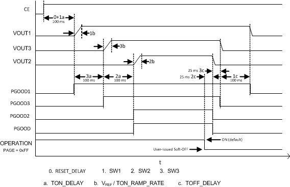
Figure 9-2 shows an internal sequencing schematic example where only switchers 1 to 3 are used for a set of timing requirements. If the internal configuration and fault handling is sufficient, and provided that the user configures the chip through SDA/SCL before placing it on a target board, then it is not necessary for a supervisory and housekeeping host controller chip like a MCU or DSP to be connected to the TPS65400. In such a case, digital terminals PGOOD, SSx/ PG, SDA/SCL, I2CALERT, and CLK_OUT can be left unconnected with no pull-ups required, during normal operation. RST_N can be tied directly to VDDD (no pull-up required). I2CADDR can be tied directly to VDDD after programming. Control line CE can be left unconnected if the chip is constantly powered after VIN is provided.
GUID-FE3191F4-AF20-4A25-B856-3472556C6A57-low.gif
PGOOD dependence disabled, switcher 4 disabled
Figure 9-2 Example Timing Diagram for Internal Sequencing