SLVSCQ9E November 2014 – March 2022 TPS65400
PRODUCTION DATA
- 1 Features
- 2 Applications
- 3 Description
- 4 Revision History
- 5 Description (continued)
- 6 Pin Configuration and Functions
- 7 Specifications
-
8 Detailed Description
- 8.1 Overview
- 8.2 Functional Block Diagrams
- 8.3
Feature Description
- 8.3.1 Startup Timing and Power Sequencing
- 8.3.2 UVLO and Precision Enables
- 8.3.3 Soft-Start and Prebiased Startup
- 8.3.4 PWM Switching Frequency Selection
- 8.3.5 Clock Synchronization
- 8.3.6 Phase Interleaving
- 8.3.7 Fault Handling
- 8.3.8 OCP for SW1 to SW4
- 8.3.9 Overcurrent Protection for SW1 to SW4 in Current Sharing Operation
- 8.3.10 Recovery on Power Loss
- 8.3.11 Feedback Compensation
- 8.3.12 Adjusting Output Voltage
- 8.3.13 Digital Interface – PMBus
- 8.3.14 Initial Configuration
- 8.4 Device Functional Modes
- 8.5 Programming
- 8.6
Register Maps
- 8.6.1
PMBus Core Commands
- 8.6.1.1 (00h) PAGE
- 8.6.1.2 (01h) OPERATION
- 8.6.1.3 (03h) CLEAR_FAULTS
- 8.6.1.4 (10h) WRITE_PROTECT
- 8.6.1.5 (11h) STORE_DEFAULT_ALL
- 8.6.1.6 (19h) CAPABILITY
- 8.6.1.7 (78h) STATUS_BYTE
- 8.6.1.8 (79h) STATUS_WORD
- 8.6.1.9 (7Ah) STATUS_VOUT
- 8.6.1.10 (80h) STATUS_MFR_SPECIFIC
- 8.6.1.11 (98h) PMBUS_REVISION
- 8.6.1.12 (ADh) IC_DEVICE_ID
- 8.6.1.13 (AEh) IC_DEVICE_REV
- 8.6.2
Manufacturer-Specific Commands
- 8.6.2.1 (D0h) USER_DATA_BYTE_00
- 8.6.2.2 (D1h) USER_DATA_BYTE_01
- 8.6.2.3 (D2h) PIN_CONFIG_00
- 8.6.2.4 (D3h) PIN_CONFIG_01
- 8.6.2.5 (D4h) SEQUENCE_CONFIG
- 8.6.2.6 (D5h) SEQUENCE_ORDER
- 8.6.2.7 (D6h) IOUT_MODE
- 8.6.2.8 (D7h) FREQUENCY_PHASE
- 8.6.2.9 (D8h) VREF_COMMAND
- 8.6.2.10 (D9h) IOUT_MAX
- 8.6.2.11 (DAh) USER_RAM_00
- 8.6.2.12 (DBh) SOFT_RESET
- 8.6.2.13 (DCh) RESET_DELAY
- 8.6.2.14 (DDh) TON_TOFF_DELAY
- 8.6.2.15 (DEh) TON_TRANSITION_RATE
- 8.6.2.16 (DFh) VREF_TRANSITION_RATE
- 8.6.2.17 (F0h) SLOPE_COMPENSATION
- 8.6.2.18 (F1h) ISENSE_GAIN
- 8.6.2.19 (FCh) DEVICE_CODE
- 8.6.1
PMBus Core Commands
- 9 Application and Implementation
- 10Power Supply Recommendations
- 11Layout
- 12Device and Documentation Support
- 13Mechanical, Packaging, and Orderable Information
Package Options
Mechanical Data (Package|Pins)
- RGZ|48
Thermal pad, mechanical data (Package|Pins)
- RGZ|48
Orderable Information
8.3.1.1 Startup Timing
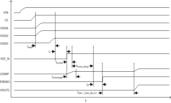
Figure 8-3 shows the startup timing of the TPS65400. Upon power-up or the rising edge of CE, the internal power rails VDDA, VDDG, and VDDD startup during the time labeled tstart. Following tstart, a delay of t1 follows (which is defined by the user through the timing of RST_N). During time tstart and t1, the COMP terminal is internally discharged through a 2-kΩ resistor. At the rising edge of RST_N, the TPS65400 begins two actions:
- The TPS65400 begins its precharge of the COMP terminal (indicated by tprecharge). The length of tprecharge needed to precharge the COMP terminal depends on the time constant of the R and C components. The internal precharge voltage source remains on even during normal operation, preventing the COMP terminal from falling below 0.6 V except during faults (OVP, OCP, and so forth).
- The TPS65400 begins its configuration sequence (indicated by tconfig), and loads parameters from the EEPROM. Parameters to be set include Vout, switching frequency, soft-start timing, and current limit.
After tconfig is complete, treset_delay begins. The length of treset_delay is user-configurable through PMBus register DCh. After treset_delay is complete, the TPS65400 begins its startup sequence. The startup sequence is EEPROM-configurable, so any of the four switchers could be the first to startup with a configurable delay. In this particular example, SW1 is configured to startup first after a delay of tSW1_TON_DELAY, which is configurable through PMBus register (DDh) TON_TOFF_DELAY.

To summarize, the length of time from rising edge of CE to soft-start of the first switcher in the sequence is:
The delays, treset_delay and tSW1_ON_DELAY, are both configurable through PMBus. The delay, tconfig, is typically 1.1 ms. The delays, t1 and t2, are determined by the user-defined timing of RST_N and ENSW1. They can both be set to 0 by pulling RST_N high before the end of tstart and ENSW1 high before the end of treset_delay. One simple way to do this would be to tie both signals to VDDD.