SBVS362C June   2020  – August 2022 TPS7B86-Q1

PRODUCTION DATA  

  1. Features
  2. Applications
  3. Description
  4. Revision History
  5. Pin Configuration and Functions
  6. Specifications
    1. 6.1 Absolute Maximum Ratings
    2. 6.2 ESD Ratings
    3. 6.3 Recommended Operating Conditions
    4. 6.4 Thermal Information
    5. 6.5 Electrical Characteristics
    6. 6.6 Switching Characteristics
    7. 6.7 Typical Characteristics
  7. Detailed Description
    1. 7.1 Overview
    2. 7.2 Functional Block Diagrams
    3. 7.3 Feature Description
      1. 7.3.1 Enable (EN)
      2. 7.3.2 Power-Good (PG)
      3. 7.3.3 Adjustable Power-Good Delay Timer (DELAY)
      4. 7.3.4 Undervoltage Lockout
      5. 7.3.5 Thermal Shutdown
      6. 7.3.6 Current Limit
    4. 7.4 Device Functional Modes
      1. 7.4.1 Device Functional Mode Comparison
      2. 7.4.2 Normal Operation
      3. 7.4.3 Dropout Operation
      4. 7.4.4 Disabled
  8. Application and Implementation
    1. 8.1 Application Information
      1. 8.1.1 Input and Output Capacitor Selection
      2. 8.1.2 Adjustable Device Feedback Resistor Selection
      3. 8.1.3 Feed-Forward Capacitor
      4. 8.1.4 Dropout Voltage
      5. 8.1.5 Reverse Current
      6. 8.1.6 Power Dissipation (PD)
        1. 8.1.6.1 Thermal Performance Versus Copper Area
        2. 8.1.6.2 Power Dissipation Versus Ambient Temperature
      7. 8.1.7 Estimating Junction Temperature
      8. 8.1.8 Power-Good
        1. 8.1.8.1 Setting the Adjustable Power-Good Delay
    2. 8.2 Typical Application
      1. 8.2.1 Design Requirements
      2. 8.2.2 Detailed Design Procedure
        1. 8.2.2.1 Input Capacitor
        2. 8.2.2.2 Output Capacitor
      3. 8.2.3 Application Curves
    3. 8.3 Power Supply Recommendations
    4. 8.4 Layout
      1. 8.4.1 Layout Guidelines
        1. 8.4.1.1 Package Mounting
        2. 8.4.1.2 Board Layout Recommendations to Improve PSRR and Noise Performance
      2. 8.4.2 Layout Examples
  9. Device and Documentation Support
    1. 9.1 Device Support
      1. 9.1.1 Device Nomenclature
    2. 9.2 Receiving Notification of Documentation Updates
    3. 9.3 Support Resources
    4. 9.4 Trademarks
    5. 9.5 Electrostatic Discharge Caution
    6. 9.6 Glossary
  10. 10Mechanical, Packaging, and Orderable Information

Package Options

Mechanical Data (Package|Pins)
Thermal pad, mechanical data (Package|Pins)
Orderable Information

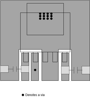
Layout Examples

Figure 8-11 DDA Package Adjusable Output
GUID-20201202-CA0I-M6LZ-N67V-8MZ3NWG1LCN1-low.gif Figure 8-12 KVU Package Fixed Outupt