SBVS363B December   2020  – November 2025 TPS7B87-Q1

PRODUCTION DATA  

  1.   1
  2. Features
  3. Applications
  4. Description
  5. Pin Configuration and Functions
  6. Specifications
    1. 5.1 Absolute Maximum Ratings
    2. 5.2 ESD Ratings
    3. 5.3 Recommended Operating Conditions
    4. 5.4 Thermal Information
    5. 5.5 Electrical Characteristics
    6. 5.6 Switching Characteristics
    7. 5.7 Typical Characteristics
  7. Detailed Description
    1. 6.1 Overview
    2. 6.2 Functional Block Diagrams
    3. 6.3 Feature Description
      1. 6.3.1 Power-Good (PG)
      2. 6.3.2 Adjustable Power-Good Delay Timer (DELAY)
      3. 6.3.3 Undervoltage Lockout
      4. 6.3.4 Thermal Shutdown
      5. 6.3.5 Current Limit
    4. 6.4 Device Functional Modes
      1. 6.4.1 Device Functional Mode Comparison
      2. 6.4.2 Normal Operation
      3. 6.4.3 Dropout Operation
      4. 6.4.4 Disabled
  8. Application and Implementation
    1. 7.1 Application Information
      1. 7.1.1 Input and Output Capacitor Selection
      2. 7.1.2 Dropout Voltage
      3. 7.1.3 Reverse Current
      4. 7.1.4 Power Dissipation (PD)
        1. 7.1.4.1 Thermal Performance Versus Copper Area
        2. 7.1.4.2 Power Dissipation Versus Ambient Temperature
      5. 7.1.5 Estimating Junction Temperature
      6. 7.1.6 Pulling Up the PG Pin to a Different Voltage
      7. 7.1.7 Power-Good
        1. 7.1.7.1 Setting the Adjustable Power-Good Delay
    2. 7.2 Typical Application
      1. 7.2.1 Design Requirements
      2. 7.2.2 Detailed Design Procedure
        1. 7.2.2.1 Input Capacitor
        2. 7.2.2.2 Output Capacitor
      3. 7.2.3 Application Curves
    3. 7.3 Power Supply Recommendations
    4. 7.4 Layout
      1. 7.4.1 Layout Guidelines
        1. 7.4.1.1 Package Mounting
        2. 7.4.1.2 Board Layout Recommendations to Improve PSRR and Noise Performance
      2. 7.4.2 Layout Examples
  9. Device and Documentation Support
    1. 8.1 Device Support
      1. 8.1.1 Device Nomenclature
    2. 8.2 Receiving Notification of Documentation Updates
    3. 8.3 Support Resources
    4. 8.4 Trademarks
    5. 8.5 Electrostatic Discharge Caution
    6. 8.6 Glossary
  10. Revision History
  11. 10Mechanical, Packaging, and Orderable Information
    1. 10.1 Mechanical Data

Package Options

Refer to the PDF data sheet for device specific package drawings

Mechanical Data (Package|Pins)
  • DDA|8
  • KVU|5
Thermal pad, mechanical data (Package|Pins)
Orderable Information

Typical Characteristics

specified at TJ = –40°C to +150°C, VIN = 13.5V, IOUT = 100μA, COUT = 2.2µF, 1mΩ < COUT ESR < 2Ω, and CIN = 1µF (unless otherwise noted)

TPS7B87-Q1 Accuracy vs
                        Temperature
 
Figure 5-1 Accuracy vs Temperature
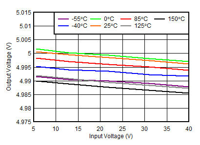
TPS7B87-Q1 Line
                        Regulation vs VIN
VOUT = 5V, IOUT = 5mA
Figure 5-3 Line Regulation vs VIN
TPS7B87-Q1 Load Regulation vs
                            IOUT
VOUT = 5V
Figure 5-5 Load Regulation vs IOUT
TPS7B87-Q1 Line Regulation at
                        100mA
COUT = 10µF, VOUT = 5V
Figure 5-7 Line Regulation at 100mA
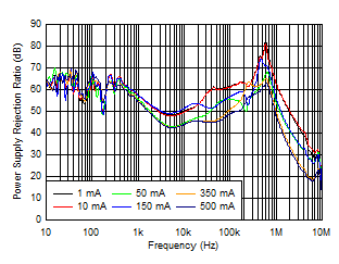
TPS7B87-Q1 PSRR vs Frequency and
                            IOUT
COUT = 10µF (X7R 50V), VOUT = 5V
Figure 5-9 PSRR vs Frequency and IOUT
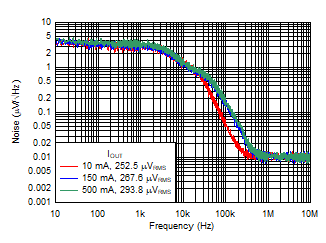
TPS7B87-Q1 Noise vs Frequency
COUT = 10µF (X7R 50V), VOUT = 3.3V
Figure 5-11 Noise vs Frequency
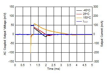
TPS7B87-Q1 Line Transients
VOUT = 5V, IOUT = 1mA, VIN = 13.5V to 45V,
slew rate = 2.7V/µs
Figure 5-13 Line Transients
TPS7B87-Q1 Load Transient, No Load to
                        100mA
VOUT = 5V, IOUT = 0mA to 100mA, slew rate = 1A/µs,
COUT = 10µF
Figure 5-15 Load Transient, No Load to 100mA
TPS7B87-Q1 Load Transient, 45mA to
                        105mA
VOUT = 5V, IOUT = 45mA to 105mA, slew rate = 0.1A/µs,
COUT = 10µF
Figure 5-17 Load Transient, 45mA to 105mA
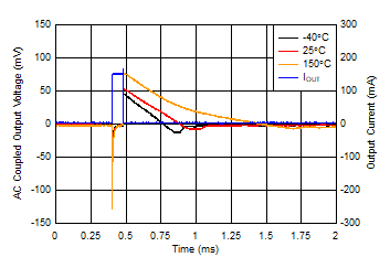
TPS7B87-Q1 Load
                        Transient, No Load to 150mA
VOUT = 5V, IOUT = 0mA to 150mA, slew rate = 1A/µs,
COUT = 10µF
Figure 5-19 Load Transient, No Load to 150mA
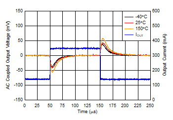
TPS7B87-Q1 Load
                        Transient, 150mA to 350mA
VOUT = 5V, IOUT = 150mA to 350mA, slew rate = 0.1A/µs,
COUT = 10µF
Figure 5-21 Load Transient, 150mA to 350mA
TPS7B87-Q1 Load
                        Transient, No Load to 500mA Rising Edge
VOUT = 5V, IOUT = 0mA to 500mA, slew rate = 1A/µs,
COUT = 10µF
 
Figure 5-23 Load Transient, No Load to 500mA Rising Edge
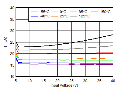
TPS7B87-Q1 Quiescent Current
                            (IQ) vs VIN
 
Figure 5-25 Quiescent Current (IQ) vs VIN
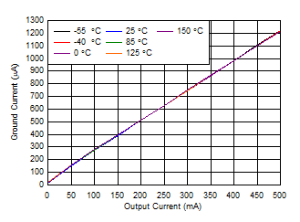
TPS7B87-Q1 Ground Current
                            (IGND) vs IOUT
 
Figure 5-27 Ground Current (IGND) vs IOUT
TPS7B87-Q1 Ground Current at
                        500µA
 
 
Figure 5-29 Ground Current at 500µA
TPS7B87-Q1 Start-Up Plot Inrush
                        Current
VIN = 13.5V, VOUT = 5V, IOUT = 150mA, COUT = 10µF
 
Figure 5-31 Start-Up Plot Inrush Current
TPS7B87-Q1 Delay
                        Pin Current vs Temperature
VDELAY = 1V
Figure 5-33 Delay Pin Current vs Temperature
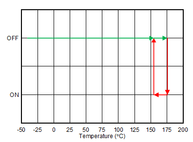
TPS7B87-Q1 Thermal Shutdown
 
Figure 5-35 Thermal Shutdown
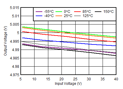
TPS7B87-Q1 Line Regulation vs
                            VIN
VOUT = 5V, IOUT = 150mA
Figure 5-2 Line Regulation vs VIN
TPS7B87-Q1 Line
                        Regulation vs VIN
VOUT = 5V, IOUT = 1mA
Figure 5-4 Line Regulation vs VIN
TPS7B87-Q1 Line Regulation at
                        50mA
COUT = 10µF, VOUT = 5V
Figure 5-6 Line Regulation at 50mA
TPS7B87-Q1 Dropout Voltage
                            (VDO) vs IOUT
VIN = 3V
Figure 5-8 Dropout Voltage (VDO) vs IOUT
TPS7B87-Q1 Noise vs Frequency
COUT = 10µF (X7R 50V), VOUT = 5V
Figure 5-10 Noise vs Frequency
TPS7B87-Q1 PSRR vs Frequency and
                            VIN
COUT = 10µF (X7R 50V), IOUT = 500mA, VOUT = 5V
Figure 5-12 PSRR vs Frequency and VIN
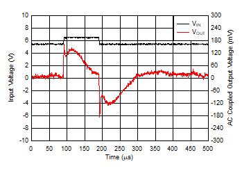
TPS7B87-Q1 Line Transients
VOUT = 5V, IOUT = 100mA, VIN = 5.5V to 6.5V,
rise time = 1µs
Figure 5-14 Line Transients
TPS7B87-Q1 Load
                        Transient, No Load to 100mA Rising Edge
VOUT = 5V, IOUT = 0mA to 100mA, slew rate = 1A/µs,
COUT = 10µF
Figure 5-16 Load Transient, No Load to 100mA Rising Edge
TPS7B87-Q1 Load
                        Transient, 45mA to 105mA Rising Edge
VOUT = 5V, IOUT = 45mA to 105mA, slew rate = 0.1A/µs,
COUT = 10µF
Figure 5-18 Load Transient, 45mA to 105mA Rising Edge
TPS7B87-Q1 Load
                        Transient, No Load to 150mA Rising Edge
VOUT = 5V, IOUT = 0mA to 150mA, slew rate = 1A/µs,
COUT = 10µF
Figure 5-20 Load Transient, No Load to 150mA Rising Edge
TPS7B87-Q1 Load
                        Transient, No Load to 500mA
VOUT = 5V, IOUT = 0mA to 500mA, slew rate = 1A/µs,
COUT = 10µF
Figure 5-22 Load Transient, No Load to 500mA
TPS7B87-Q1 Output Current Limit vs
                        Temperature
VIN = VOUT + 1V, VOUT = 90% × VOUT(NOM)
Figure 5-24 Output Current Limit vs Temperature
TPS7B87-Q1 Quiescent Current
                            (IQ) vs VIN
VOUT = 5V
Figure 5-26 Quiescent Current (IQ) vs VIN
TPS7B87-Q1 Ground Current at 100mA
 
Figure 5-28 Ground Current at 100mA
TPS7B87-Q1 PG Threshold vs
                        Temperature
 
Figure 5-30 PG Threshold vs Temperature
TPS7B87-Q1 Undervoltage Lockout
                        (UVLO) Threshold vs Temperature
 
Figure 5-32 Undervoltage Lockout (UVLO) Threshold vs Temperature
TPS7B87-Q1 Output Voltage vs Injected
                        Current
 
Figure 5-34 Output Voltage vs Injected Current
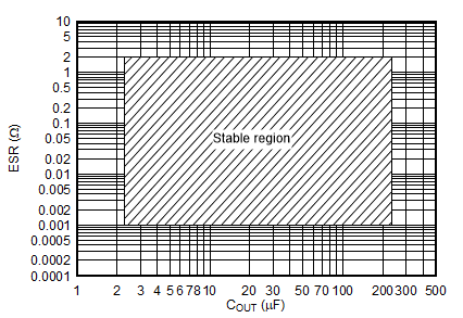
TPS7B87-Q1 Stability, ESR vs
                            COUT
 
Figure 5-36 Stability, ESR vs COUT