SLVSBC6C March 2013 – December 2019 TPS84A20
PRODUCTION DATA.
- 1 Features
- 2 Applications
- 3 Description
- 4 Revision History
- 5 Ordering Information
- 6 Specifications
- 7 Device Information
- 8 Typical Characteristics (PVIN = VIN = 12 V)
- 9 Typical Characteristics (PVIN = VIN = 5 V)
- 10Typical Characteristics (PVIN = 3.3 V, VIN = 5 V)
-
11Application Information
- 11.1 Adjusting the Output Voltage
- 11.2 Capacitor Recommendations for the TPS84A20 Power Supply
- 11.3 Transient Response
- 11.4 Transient Waveforms
- 11.5 Application Schematics
- 11.6 VIN and PVIN Input Voltage
- 11.7 3.3 V PVIN Operation
- 11.8 Power Good (PWRGD)
- 11.9 Light Load Efficiency (LLE)
- 11.10 SYNC_OUT
- 11.11 Parallel Operation
- 11.12 Power-Up Characteristics
- 11.13 Pre-Biased Start-Up
- 11.14 Remote Sense
- 11.15 Thermal Shutdown
- 11.16 Output On/Off Inhibit (INH)
- 11.17 Slow Start (SS/TR)
- 11.18 Overcurrent Protection
- 11.19 Synchronization (CLK)
- 11.20 Sequencing (SS/TR)
- 11.21 Programmable Undervoltage Lockout (UVLO)
- 11.22 Layout Considerations
- 11.23 EMI
- 12Device and Documentation Support
- 13Mechanical, Packaging, and Orderable Information
Package Options
Refer to the PDF data sheet for device specific package drawings
Mechanical Data (Package|Pins)
- RVQ|42
Thermal pad, mechanical data (Package|Pins)
Orderable Information
11.23 EMI
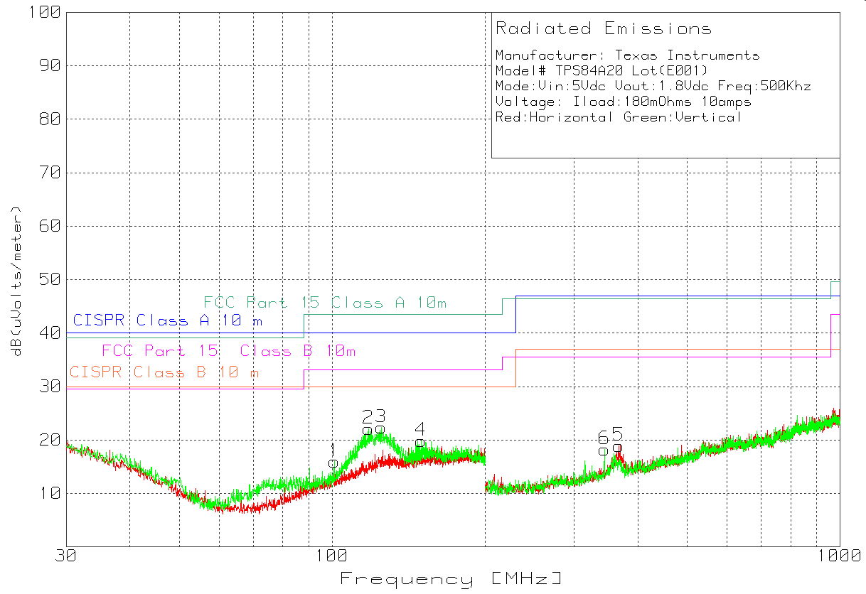
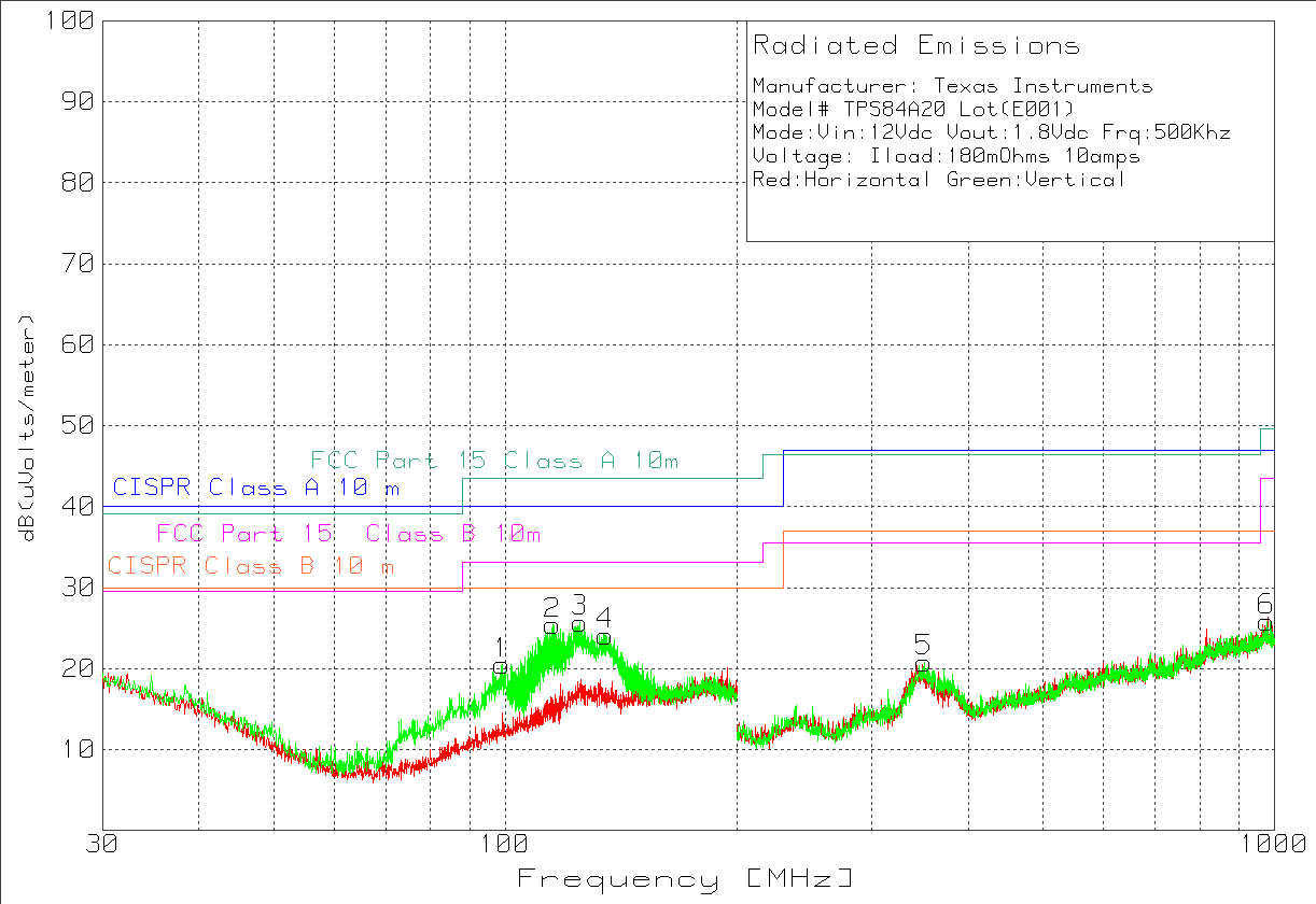
The TPS84A20 is compliant with EN55022 Class B radiated emissions. Figure 49 and Figure 50 show typical examples of radiated emissions plots for the TPS84A20 operating from 5V and 12V respectively. Both graphs include the plots of the antenna in the horizontal and vertical positions.
 Figure 49. Radiated Emissions 5-V Input, 1.8-V Output, 10-A Load (EN55022 Class B)
  Figure 50. Radiated Emissions 12-V Input, 1.8-V Output, 10-A Load (EN55022 Class B)