SLVSBC6C March 2013 – December 2019 TPS84A20
PRODUCTION DATA.
- 1 Features
- 2 Applications
- 3 Description
- 4 Revision History
- 5 Ordering Information
- 6 Specifications
- 7 Device Information
- 8 Typical Characteristics (PVIN = VIN = 12 V)
- 9 Typical Characteristics (PVIN = VIN = 5 V)
- 10Typical Characteristics (PVIN = 3.3 V, VIN = 5 V)
-
11Application Information
- 11.1 Adjusting the Output Voltage
- 11.2 Capacitor Recommendations for the TPS84A20 Power Supply
- 11.3 Transient Response
- 11.4 Transient Waveforms
- 11.5 Application Schematics
- 11.6 VIN and PVIN Input Voltage
- 11.7 3.3 V PVIN Operation
- 11.8 Power Good (PWRGD)
- 11.9 Light Load Efficiency (LLE)
- 11.10 SYNC_OUT
- 11.11 Parallel Operation
- 11.12 Power-Up Characteristics
- 11.13 Pre-Biased Start-Up
- 11.14 Remote Sense
- 11.15 Thermal Shutdown
- 11.16 Output On/Off Inhibit (INH)
- 11.17 Slow Start (SS/TR)
- 11.18 Overcurrent Protection
- 11.19 Synchronization (CLK)
- 11.20 Sequencing (SS/TR)
- 11.21 Programmable Undervoltage Lockout (UVLO)
- 11.22 Layout Considerations
- 11.23 EMI
- 12Device and Documentation Support
- 13Mechanical, Packaging, and Orderable Information
Package Options
Refer to the PDF data sheet for device specific package drawings
Mechanical Data (Package|Pins)
- RVQ|42
Thermal pad, mechanical data (Package|Pins)
Orderable Information
11.18 Overcurrent Protection
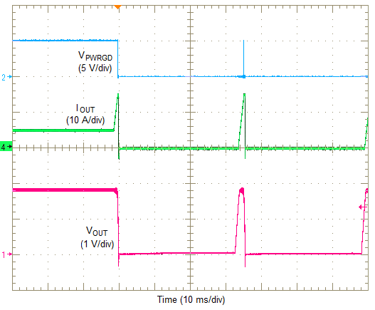
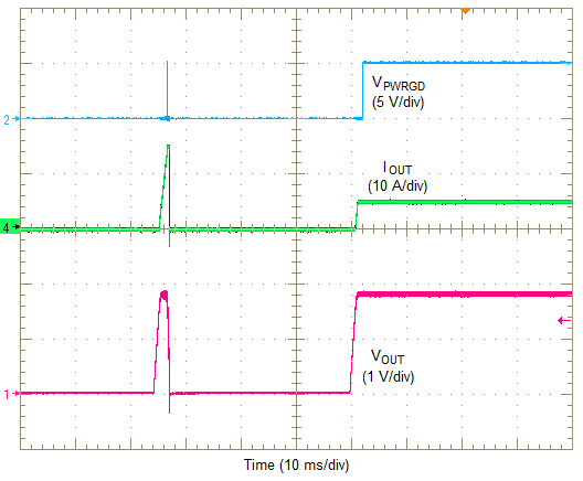
For protection against load faults, the TPS84A20 incorporates output overcurrent protection. The overcurrent protection mode can be selected using the OCP_SEL pin. Leaving the OCP_SEL pin open selects hiccup mode and connecting it to AGND selects cycle-by-cycle mode. In hiccup mode, applying a load that exceeds the overcurrent threshold of the regulator causes the regulated output to shut down. Following shutdown, the module periodically attempts to recover by initiating a soft-start power-up as shown in Figure 33. This is described as a hiccup mode of operation, whereby the module continues in a cycle of successive shutdown and power up until the load fault is removed. During this period, the average current flowing into the fault is significantly reduced which reduces power dissipation. Once the fault is removed, the module automatically recovers and returns to normal operation as shown in Figure 34.
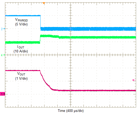
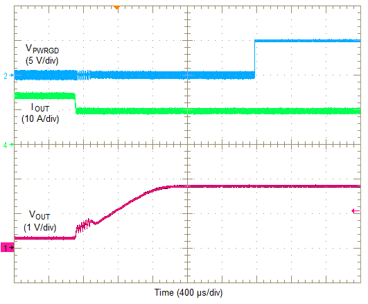
In cycle-by-cycle mode, applying a load that exceeds the overcurrent threshold of the regulator limits the output current and reduces the output voltage as shown in Figure 35. During this period, the current flowing into the fault remains high causing the power dissipation to stay high as well. Once the overcurrent condition is removed, the output voltage returns to the set-point voltage as shown in Figure 36.
 Figure 33. Overcurrent Limiting (Hiccup)
  Figure 35. Overcurrent Limiting (Cycle-by-Cycle)
  Figure 34. Removal of Overcurrent (Hiccup)
  Figure 36. Removal of Overcurrent (Cycle-by-Cycle)