SLUSEP8 January 2022 TPSM5D1806E
PRODUCTION DATA
- 1 Features
- 2 Applications
- 3 Description
- 4 Revision History
- 5 Pin Configuration and Functions
- 6 Specifications
-
7 Detailed Description
- 7.1 Overview
- 7.2 Functional Block Diagram
- 7.3
Feature Description
- 7.3.1 Adjustable Output Voltage
- 7.3.2 Frequency Selection
- 7.3.3 Minimum and Maximum Input Voltage
- 7.3.4 Recommended Settings
- 7.3.5 Device Mode Configuration
- 7.3.6 Input Capacitors
- 7.3.7 Minimum Required Output Capacitance
- 7.3.8 Ambient Temperature Versus Total Power Dissipation
- 7.3.9 Remote Sense
- 7.3.10 Enable (EN) and Undervoltage Lockout (UVLO)
- 7.3.11 Soft Start
- 7.3.12 Power Good
- 7.3.13 Safe Start-Up into Pre-Biased Outputs
- 7.3.14 BP5
- 7.3.15 Overcurrent Protection
- 7.3.16 Thermal Shutdown
- 7.4 Device Functional Modes
- 8 Application and Implementation
- 9 Power Supply Recommendations
- 10Layout
- 11Device and Documentation Support
- 12Mechanical, Packaging, and Orderable Information
Package Options
Mechanical Data (Package|Pins)
- RDB|51
Thermal pad, mechanical data (Package|Pins)
Orderable Information
3 Description
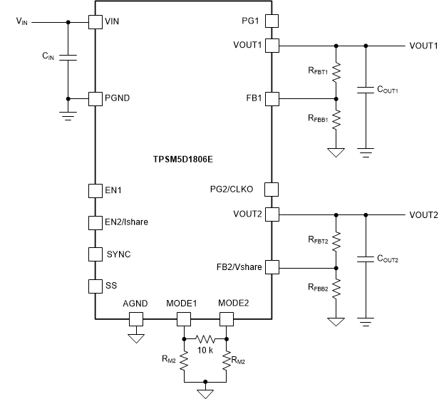
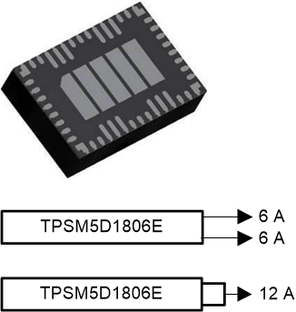
The TPSM5D1806E dual 6-A output power module is a highly integrated and flexible DC-DC power supply packaged in a compact 8-mm × 5.5-mm × 1.8-mm QFN package. The input voltage range of 4.5 V to 15 V allows conversion from a wide intermediate bus as well as standard 5-V and 12-V rails. The two 6-A outputs can be configured independently for two separate power rails or combined for a single 2-phase, 12-A output.
The low-profile, 51-pin QFN package with optimal package layout enhances thermal performance. The enhanced temperature performance of –55°C enables aerospace applications in environments such as outside cabin-mounted modules or flight control units. The package footprint has all signal pins accessible from the perimeter and large thermal pads beneath the device for simple layout and easy handling in manufacturing.
The integrated power design eliminates the loop compensation and magnetics part selection from the design process. The device offers independent enable control and power-good signal for each output. Switching frequency and phase offsetting can be configured using pin-strapping. The device also offers overcurrent and thermal shutdown protection.
| DEVICE NUMBER | PACKAGE(1) | BODY SIZE (NOM) |
|---|---|---|
| TPSM5D1806E | QFN | 8 mm × 5.5 mm × 1.8 mm |
 Dual Output Simplified
Schematic
 Output Configurations