SLUSEO6B may 2023 – july 2023 TPSM843B22
PRODUCTION DATA
- 1
- 1 Features
- 2 Applications
- 3 Description
- 4 Revision History
- 5 Pin Configuration and Functions
- 6 Specifications
-
7 Detailed Description
- 7.1 Overview
- 7.2 Functional Block Diagram
- 7.3
Feature Description
- 7.3.1 VIN Pins and VIN UVLO
- 7.3.2 Internal Bypassing (BP5)
- 7.3.3 Enable and Adjustable UVLO
- 7.3.4 Switching Frequency Selection
- 7.3.5 Switching Frequency Synchronization to an External Clock
- 7.3.6 Remote Sense Amplifier and Adjusting the Output Voltage
- 7.3.7 Loop Compensation Guidelines
- 7.3.8 Soft Start and Prebiased Output Start-up
- 7.3.9 MSEL Pin
- 7.3.10 Power Good (PG)
- 7.3.11 Output Overload Protection
- 7.3.12 Output Overvoltage and Undervoltage Protection
- 7.3.13 Overtemperature Protection
- 7.3.14 Output Voltage Discharge
- 7.4 Device Functional Modes
-
8 Application and Implementation
- 8.1 Application Information
- 8.2
Typical Applications
- 8.2.1
1.0-V Output, 1-MHz Application
- 8.2.1.1 Design Requirements
- 8.2.1.2
Detailed Design Procedure
- 8.2.1.2.1 Switching Frequency
- 8.2.1.2.2 Output Inductor Selection
- 8.2.1.2.3 Output Capacitor
- 8.2.1.2.4 Input Capacitor
- 8.2.1.2.5 Adjustable Undervoltage Lockout
- 8.2.1.2.6 Output Voltage Resistors Selection
- 8.2.1.2.7 Bootstrap Capacitor Selection
- 8.2.1.2.8 BP5 Capacitor Selection
- 8.2.1.2.9 PG Pullup Resistor
- 8.2.1.2.10 Current Limit Selection
- 8.2.1.2.11 Soft-Start Time Selection
- 8.2.1.2.12 Ramp Selection and Control Loop Stability
- 8.2.1.2.13 MSEL Pin
- 8.2.1.3 Application Curves
- 8.2.1
1.0-V Output, 1-MHz Application
- 8.3 Power Supply Recommendations
- 8.4 Layout
- 9 Device and Documentation Support
- 10Mechanical, Packaging, and Orderable Information
Package Options
Mechanical Data (Package|Pins)
- RDG|25
Thermal pad, mechanical data (Package|Pins)
Orderable Information
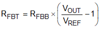
7.3.6 Remote Sense Amplifier and Adjusting the Output Voltage
Remote sensing of the output voltage is provided through a dedicated high speed, low offset instrumentation type amplifier. Connect the output voltage setting resistive divider described below from the output voltage sensing point to the GOSNS pin. The center point is to be connected to the FB pin. Note the GOSNS pin is to be tied to the converter output voltage return at a location near to the load.
The output voltage is programmed with a resistor divider from the converter output (VOUT) to the FB pin as shown in Figure 7-5. Use 1% tolerance or better divider resistors.
 Figure 7-5 FB Resistor Divider
Starting with a fixed value for the bottom resistor, typically 10 kΩ, use Equation 3 to calculate the top resistor in the divider.