SLWS245B May 2014 – February 2017 TRF3722
PRODUCTION DATA.
- 1 Features
- 2 Applications
- 3 Description
- 4 Revision History
- 5 Pin Configuration and Functions
-
6 Specifications
- 6.1 Absolute Maximum Ratings
- 6.2 ESD Ratings
- 6.3 Recommended Operating Conditions
- 6.4 Thermal Information
- 6.5 Electrical Characteristics
- 6.6 Typical Characteristics
- 6.7 Typical Characteristics - Output Power
- 6.8 Typical Characteristics - Gain
- 6.9 Typical Characteristics - OIP3
- 6.10 Typical Characteristics - OIP2
- 6.11 Typical Characteristics - OP1dB
- 6.12 Typical Characteristics - Noise
- 6.13 Typical Characteristics - Unadjusted CF
- 6.14 Typical Characteristics - Unadjusted SBS
- 6.15 Typical Characteristics - LO Harmonic
- 6.16 Typical Characteristics - BB Harmonic
- 6.17 Typical Characteristics - RF Output Return Loss
- 6.18 Typical Characteristics - PLL/VCO
- 6.19 Typical Characteristics - Current Consumption
- 6.20 Typical Characteristics - Power Dissipation
- 7 Parameter Measurement Information
- 8 Detailed Description
- 9 Application and Implementation
- 10Power Supply Recommendations
- 11Layout
- 12Device and Documentation Support
- 13Mechanical, Packaging, and Orderable Information
Package Options
Mechanical Data (Package|Pins)
- RGZ|48
Thermal pad, mechanical data (Package|Pins)
- RGZ|48
Orderable Information
7 Parameter Measurement Information
7.1 Serial Interface Timing Diagram
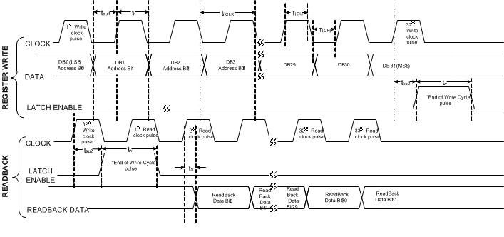
The TRF3722 features a four-wire serial programming interface (4WI) that controls an internal 32-bit shift register with seven parallel registers. There are total of three signals that must be applied: the clock (CLK), the serial data (DATA), and the latch enable (LE). The fouth signal is the read back (RDBK) signal. The serial data (DB0-DB31) are loaded least significant bit (LSB) first, and read on the rising edge of the CLK. LE is asynchronous to the CLK signal; at its rising edge, the data in the shift register are loaded into the selected internal register. Figure 130 shows the timing diagram the 4WI. Table 1 lists the 4WI timing for the write operation.
 Figure 130. 4WI Writing Timing Diagram
Table 1. 4WI Timing for Write Operation
| MIN | TYP | MAX | UNIT | ||
|---|---|---|---|---|---|
| th | Hold time, data to clock | 20 | ns | ||
| tSU1 | Setup time, data to clock | 20 | ns | ||
| tCH | Clock low duration | 20 | ns | ||
| tCL | Clock High duration | 20 | ns | ||
| tSU2 | Setup time, clock to enable | 20 | ns | ||
| tCLK | Clock period | 50 | ns | ||
| tW | Enable Time | 50 | ns | ||
| tSU3 | Setup time, Latch to Data | 70 | ns | ||
TRF3722 integrates 7 registers: Register 0 (000) to Register 6 (110). Registers 1 through 6 are used to set-up and control the TRF3722 functionalities, while register 0 is used for the read-back function. Each read-back is composed by two phases: writing followed by the actual reading of the internal data. This is shown in the timing diagram in Figure 131.
 Figure 131. 4WI Read-Back Timing Diagram
During the writing phase a command is sent to TRF3722 register 0 to set it in read-back mode and to specify which register is to be read. In the proper reading phase, at each rising clock edge, the internal data is transferred into the RDBK pin and can be read at the following falling edge (LSB first). The first clock after the LE goes high (end of writing cycle) is idle and the following 32 clocks pulses will transfer the internal register content to the RDBK pin. Table 2 shows the Readback timing.
Table 2. 4WI Timing for Readback Timing
| MIN | TYP | MAX | UNIT | COMMENT | ||
|---|---|---|---|---|---|---|
| th | Hold time, data to clock | 20 | ns | |||
| tSU1 | Setup time, data to clock | 20 | ns | |||
| tCH | Clock low duration | 20 | ns | |||
| tCL | Clock High duration | 20 | ns | |||
| tSU2 | Setup time, clock to enable | 20 | ns | |||
| tSU3 | Setup time, enable to Readback clock | 20 | ns | |||
| td | Delay time, clock to Readback data output | 10 | ||||
| tW | Enable Time | 50 | ns | Equals Clock period | ||
| t(CLK) | Clock period | 50 | ns | |||